
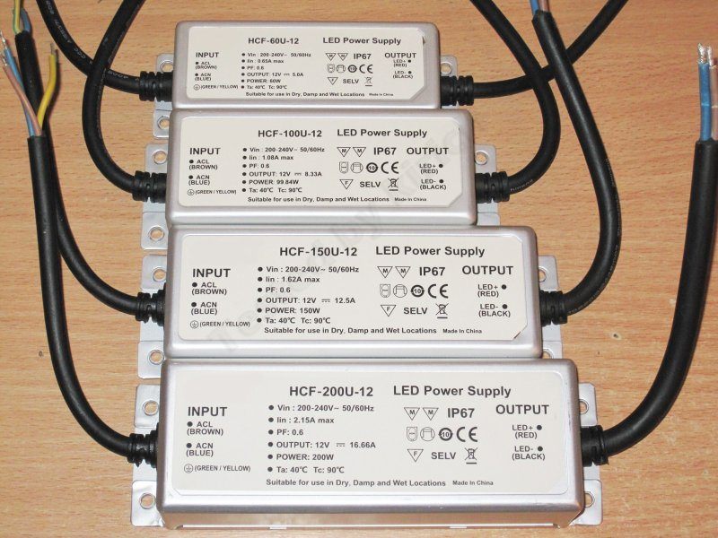
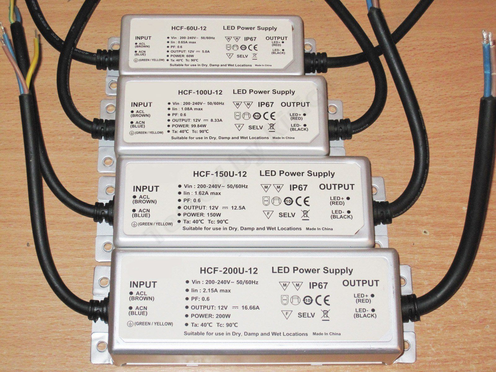
Four 12 V power supplies: 60, 100, 150, and 200 W
I received several test samples from one of the factories. They were originally designed to be sealed, but we asked them to send the units without potting compound so we could test them “bare” and take a look inside.
As a reminder, if you want to stay up to date with new posts on the blog, I recommend following me on Instagram. I’ll post notifications about every new article there, and maybe write about other interesting things too - link to my account
You can also subscribe to updates and new articles on the Telegram channel - https://t.me/KirichBlog
This review will be fairly brief. I tried to bring all the tests in line with one “standard”; I think that will make things more convenient for you and easier for me.
I’ve actually had these for a very long time. At one point I even changed my mind about testing them and writing a review, but curiosity got the better of me—and it turned out to be worth it.
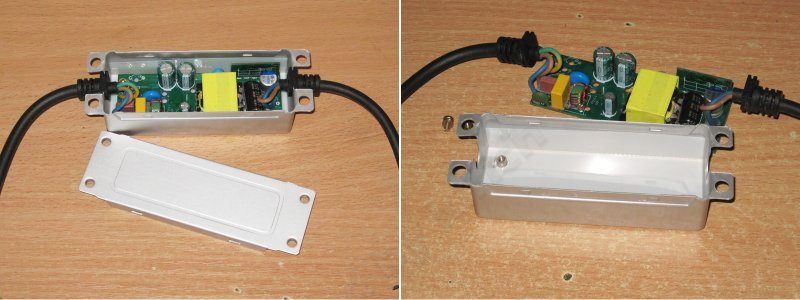
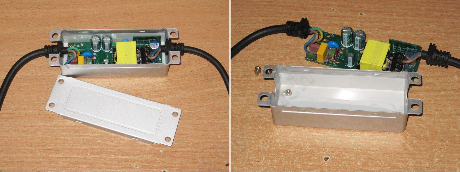
All the models come in metal enclosures, but these aren’t made from standard extruded profiles or U-shaped cases. They’re more like little trays with snap-on lids. Pretty neat and convenient :)
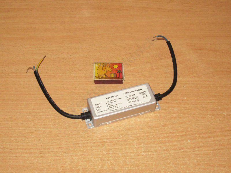
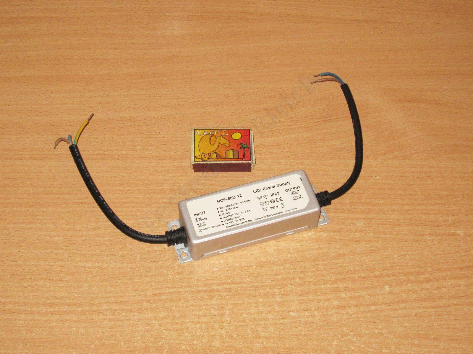
All the power supplies also come with connection cables. They’re not very long, but the wire gauge is perfectly adequate. They are pretty stiff, though, especially the output cable on the 200 W model.
These are 12 V power supplies rated at 60, 100, 150, and 200 W—in other words, the most common ratings.
As usual, let’s start with the smallest model: 60 W, or 5 A.
The board is secured inside with a couple of screws, but that’s fine considering the unit is normally potted. There’s also a plastic insulating sheet.
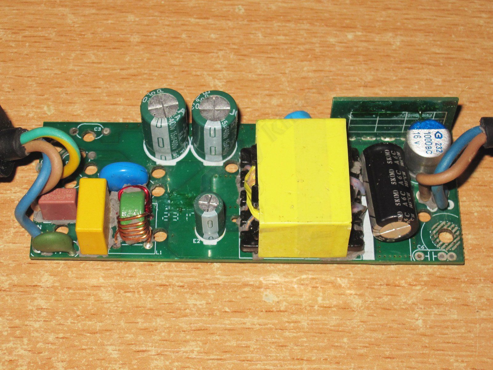
It looks reasonably tidy, though some areas seem oddly empty while others look a bit strange.
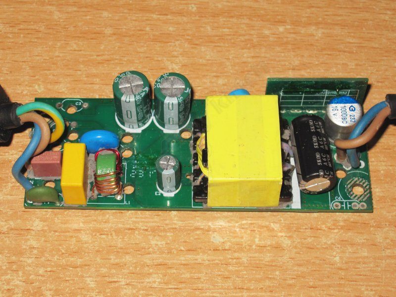
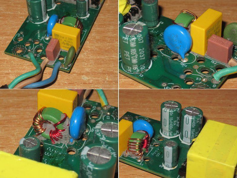
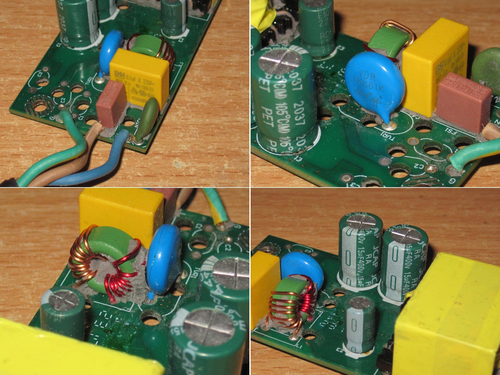
1. There’s an input EMI filter and a thermistor. It’s basic, but the essentials are there.
2. There’s even a varistor, rated for 560 V (about 395 V RMS), so it won’t provide overvoltage protection; it’s more likely there to suppress transient spikes.
3. Common-mode input choke.
4. There are two 15 µF capacitors on the input. In my opinion, that’s far too little.
While taking photos of the power supply, I realized what had seemed strange to me. Usually, in cases like this, the manufacturer sends units before they’re potted—that’s understandable and logical. But I was a bit stunned to find that this unit had been potted and then carefully cleaned out. I’m genuinely shocked.
So the person who sent these to me and I suspect that they’re actually made by another factory, and this one simply resells them.
Of course, that’s not a fact. But it seems less likely to me that someone took a finished unit, opened it up, and cleaned it out completely. What do you think? What are the possibilities?
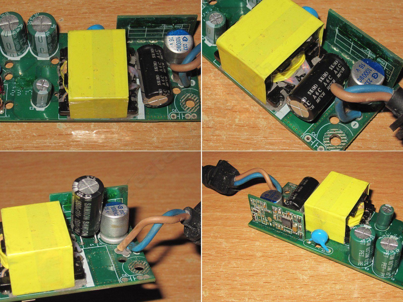
1. The transformer looks perfectly adequate for the claimed 60 W, if not more.
2. And it uses litz wire—nice.
3. A small but welcome detail: the output has not only a polymer capacitor, but also a regular one right next to it, and it’s a decent Samxon part.
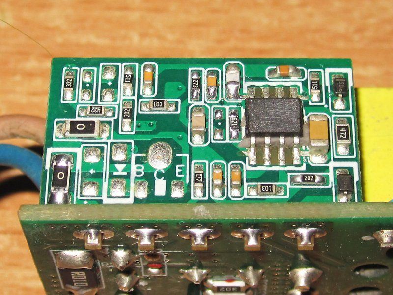
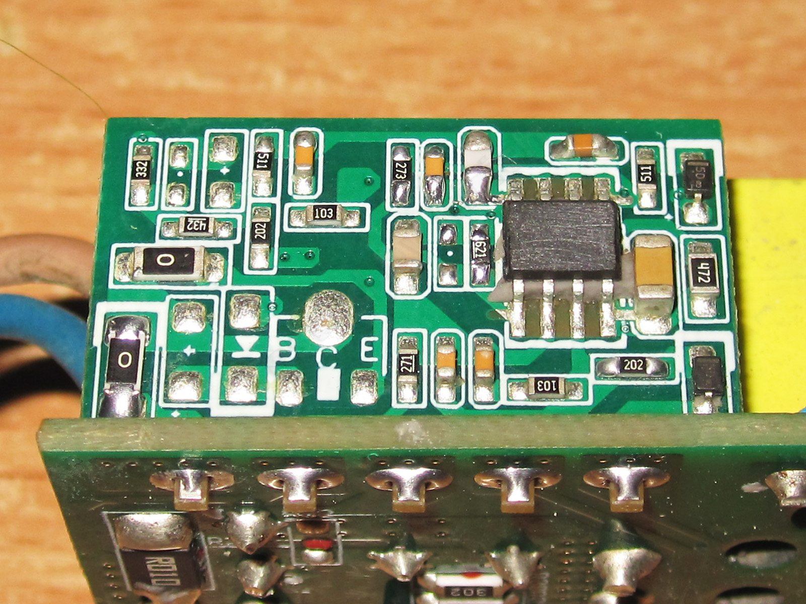
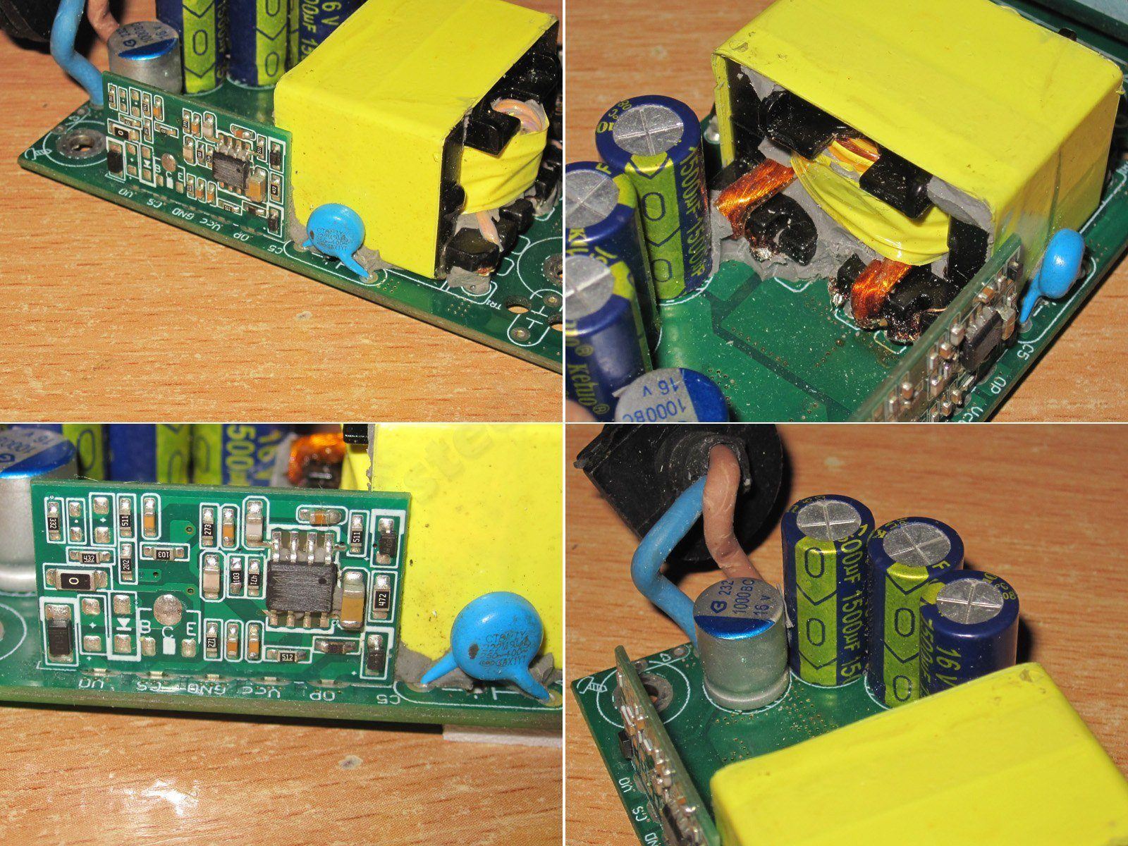
4. There’s a Y capacitor and... some kind of little board. Hmm...

Sure, I’ve seen power supplies with various submodules, but this clearly isn’t Bluetooth or Wi-Fi—it wouldn’t work inside a metal enclosure. There’s no mention of anything fancy like smart regulation, but the little board is there, and it clearly isn’t a TL431.
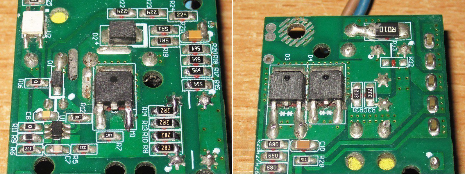
The chip marking has been rubbed off. I’d guess it’s an LM358, but I’m not certain. There are other possibilities, and judging by the unpopulated spots, the board may have been designed for models other than the 12 V version too, since there’s space for a basic voltage regulator.
I have no safety concerns, at least nothing obviously wrong stands out.
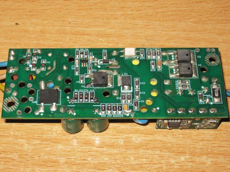
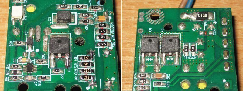
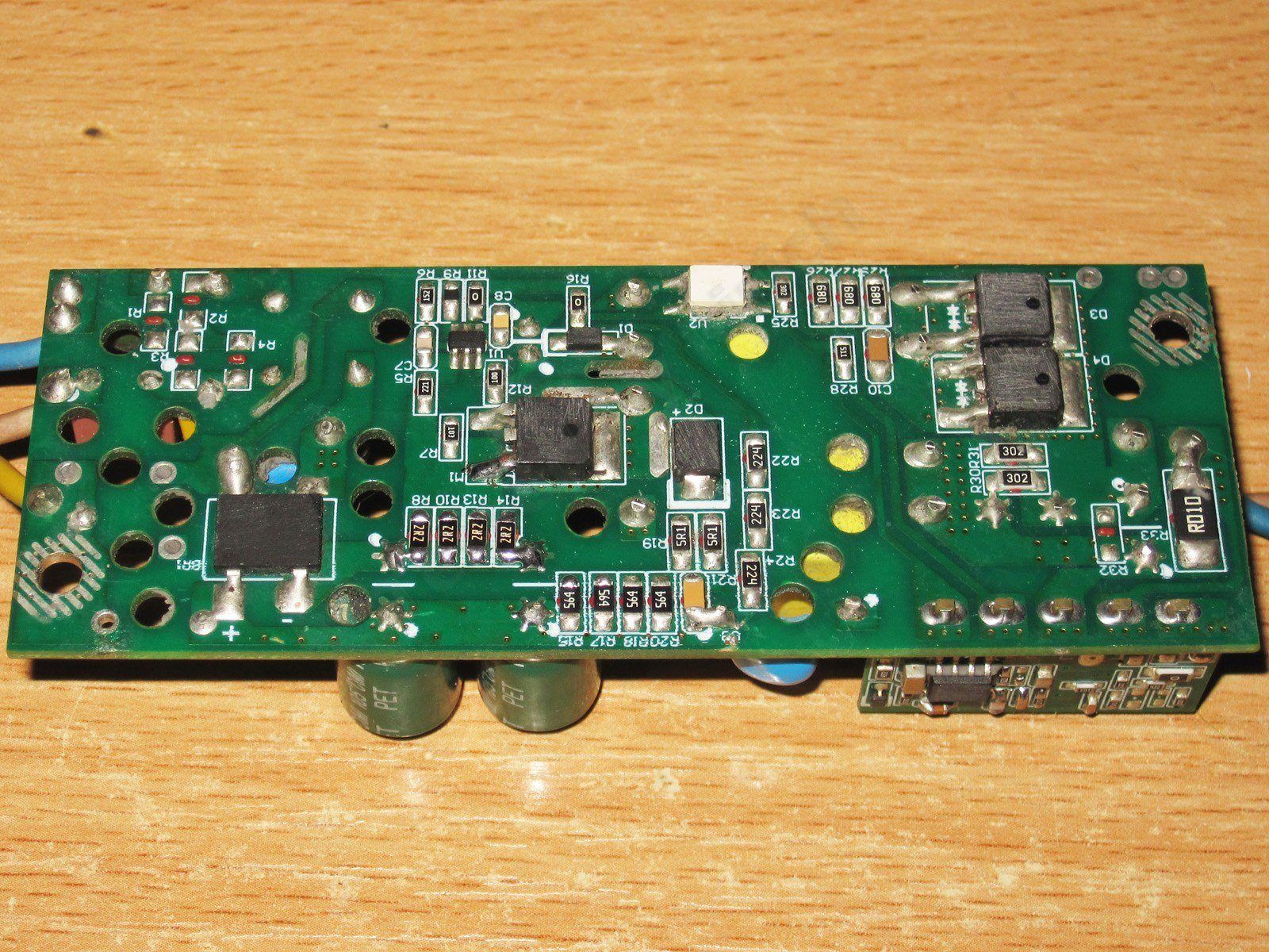
1. It’s curious that they’ve rubbed off the markings on every semiconductor, right down to the diodes. Paranoia? I think they did it specifically for the test samples.
2. On the output there are two diodes and... a shunt. Well, that’s clearly something new. I’ve seen this kind of thing before, of course, but it’s so rare I can hardly put it into words...
The first thing you notice is also the absence of the usual TL431, which gives me a few ideas.
First, the manufacturer has made some kind of universal module that handles the power supply’s entire feedback loop.
The module monitors not only voltage but also current. There’s also current monitoring on the primary side, which means the module is designed to operate in CC mode.
Why is that useful?
First, it provides overload protection—and better than monitoring the primary side, since that essentially limits power rather than output current.
Second, this design lets you connect power supplies in parallel, and they don’t even have to be the same power rating. You could use a 150 W unit and a 200 W unit to get, essentially, a 350 W power supply. Of course, this still needs to be tested, but everything points to that being possible. It depends on the current threshold and whether there’s a genuine CC mode.
All this raises the question: what chip could this be? I suspect it’s an AP4310, a dual op-amp combined with a voltage reference. I’ve come across it in this UPS
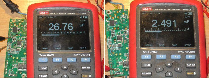
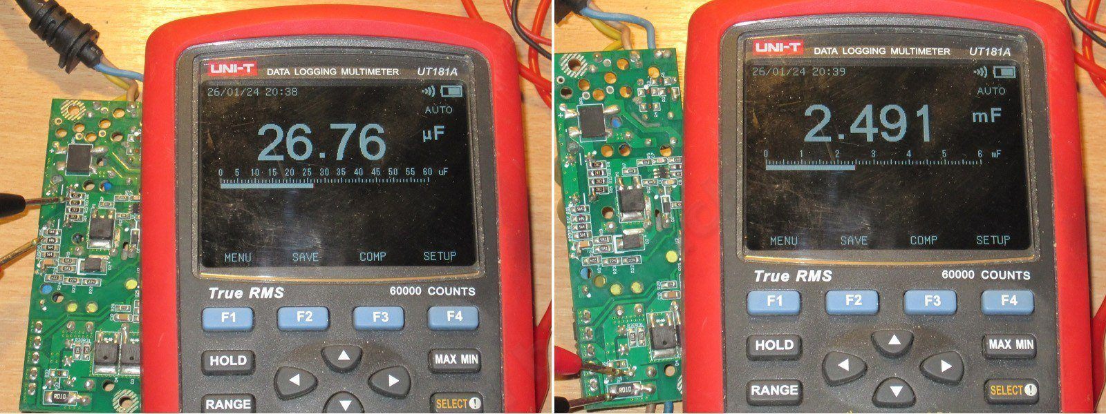
The actual capacitance of the input capacitors is close to the stated value, so no issues there. But the capacitance itself is questionable: even 30 µF is too little for a 60 W power supply, and that’s true even at 230 V, let alone 115 V, although the manufacturer specifies an operating range starting at 200 V. Still, it’s too little. Sure, it’ll work, but first, 100 Hz ripple will increase; second, the capacitors’ service life will be reduced; and third, if you install this power supply outdoors, as it’s clearly intended to be, freezing temperatures will cause real trouble.
No particular complaints about the output, especially since there’s also a polymer capacitor.
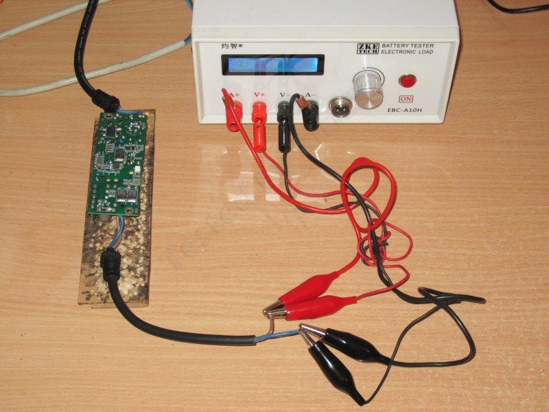
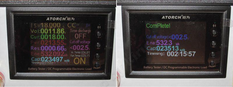
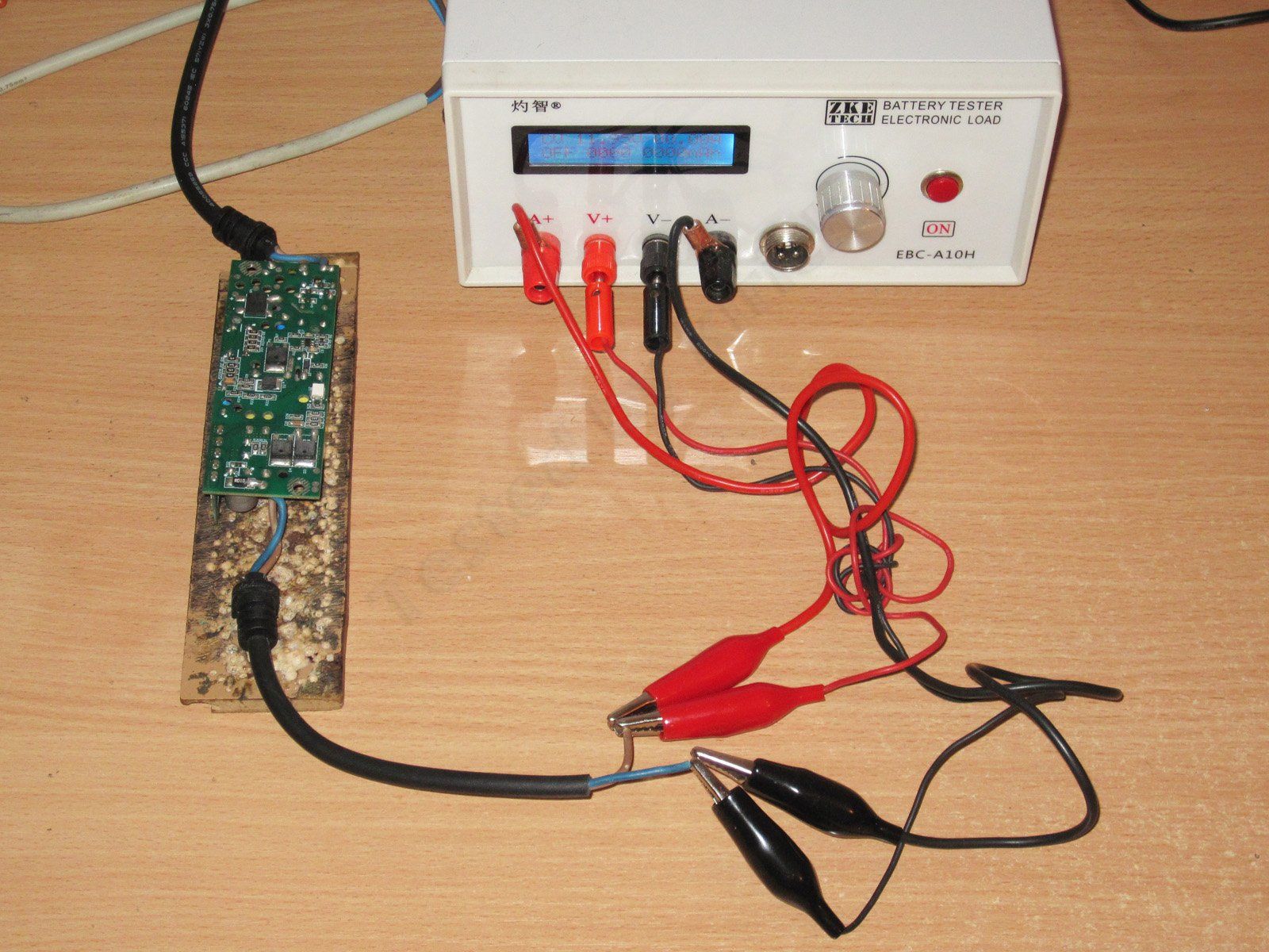
I used an EBC-A10H electronic load for testing. The board was simply lying on the table, and, as always, there’s a catch: it’s designed to be potted with compound, so it usually cools less effectively in this state. Though perhaps that actually makes for a more realistic test.
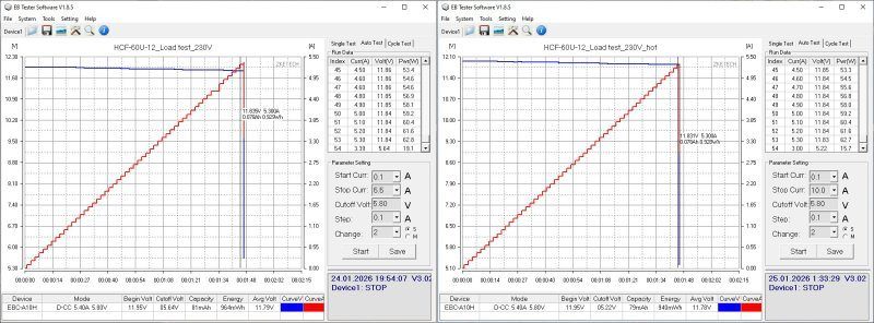
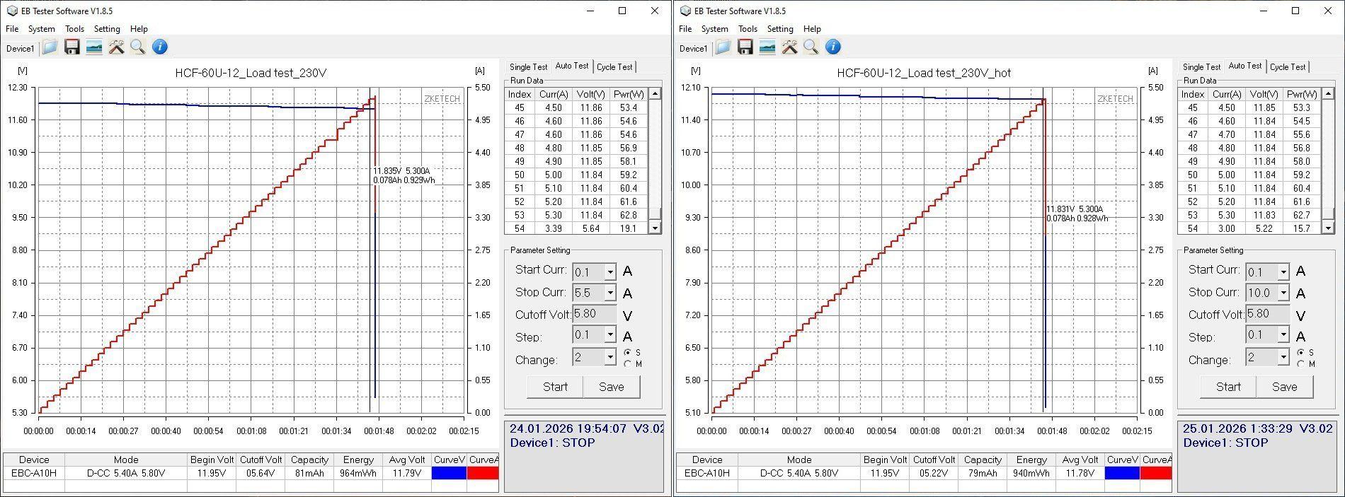
The test showed that the protection is set to a current of about 5.3 A, and this doesn’t depend on the power supply’s temperature. Someone will surely ask: where’s the CC mode?
Let me explain again: power supplies that operate in CC mode should be tested with an electronic load in CV mode, and vice versa. If you load a power supply with CC mode using an electronic load in CC mode, the current limiting should work exactly as it does here—that is, the voltage should drop to zero.
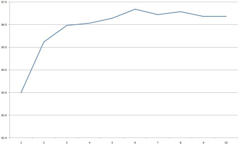
I measured efficiency from 0.5 to 5 A in 0.5 A increments, and in my opinion it’s pretty good for a power supply like this.
Ripple with no load and at 1.5, 3, and 5 A.
I wouldn’t call it low, but it’s not high either. I think the polymer capacitor helps a lot, so adding it was the right call.
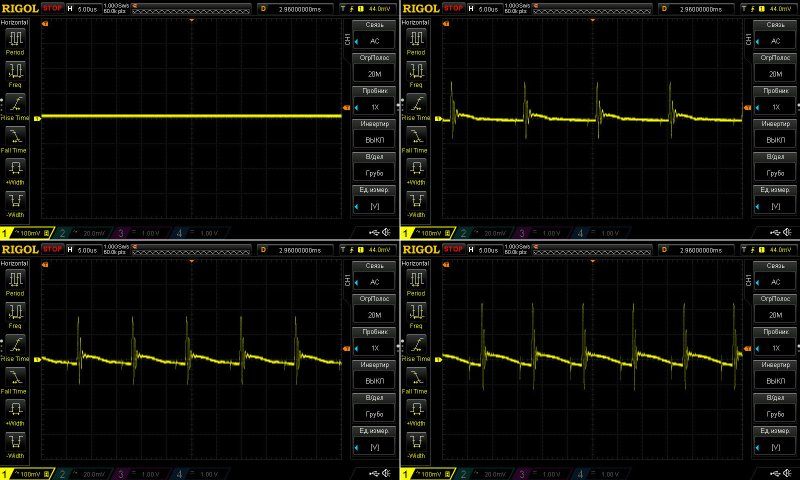
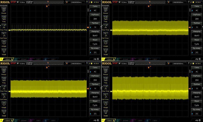
There’s almost no 100 Hz ripple despite the low input capacitance, but that’s probably thanks to the circuit design and the 230 V input.
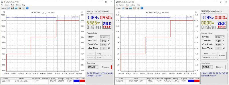
The load test was run in three modes: 1.5, 3, and 4.5 A. To be honest, I don’t remember why I capped it at 4.5 A instead of 5.
The output voltage does vary with load, but not by much. Some of that is due to the voltage drop in the output cable. There’s no temperature dependence.
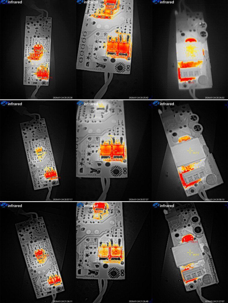
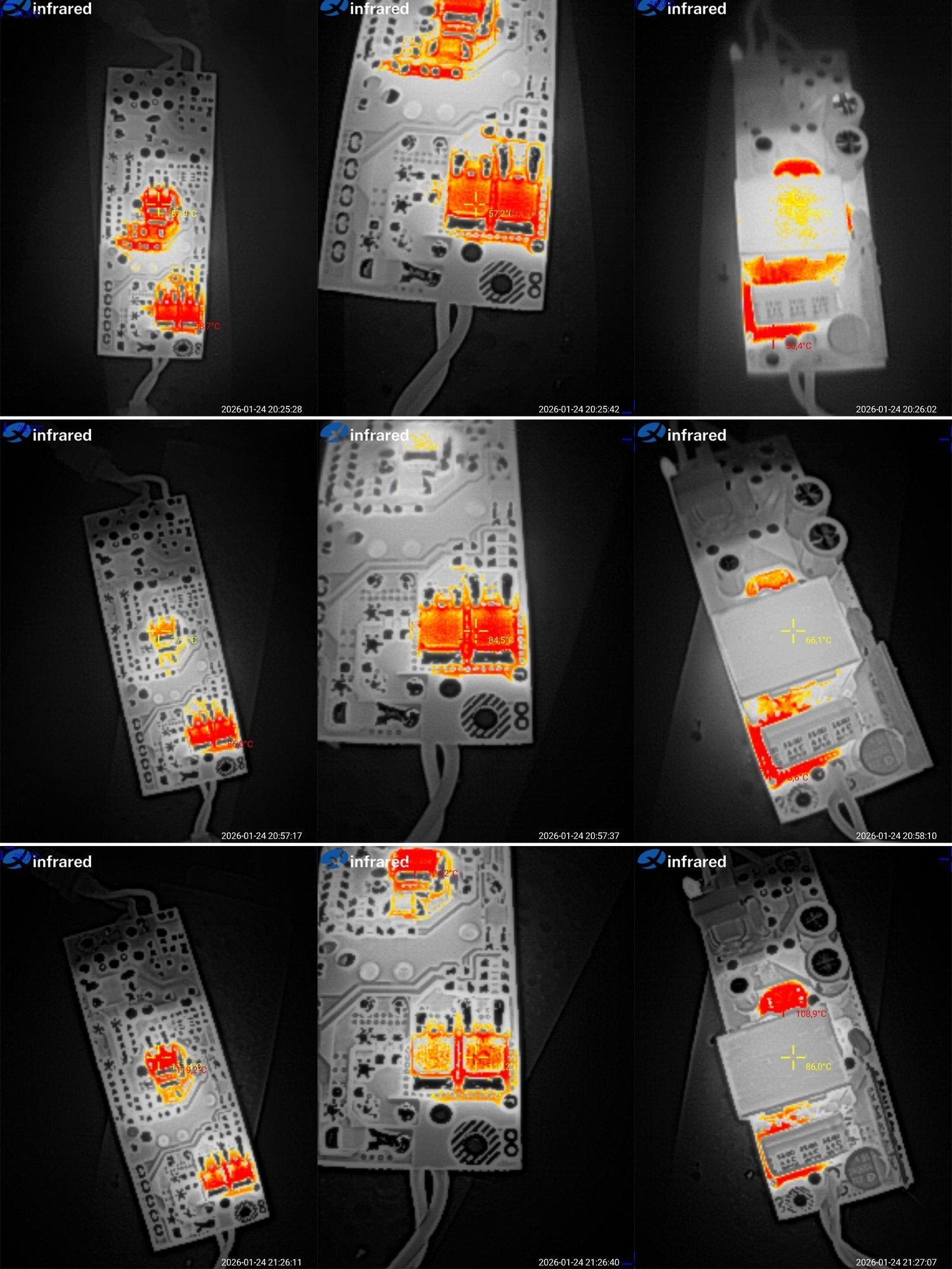
Temperatures in all three modes. There’s no point commenting on the 1.5 A results, so I’ll go straight to 3 and 4.5 A.
At 3 A: transistor 77 °C, diodes around 85 °C, transformer 66 °C—excellent.
At 4.5 A: transistor 120 °C, too high; diodes 120 °C, also rather high; transformer 86 °C, perfectly fine.
Yes, the transistor and diode temperatures are on the high side, but I think it’s worth bearing in mind that air usually carries heat away less effectively than potting compound. So I’d expect temperatures to be lower once it’s in the enclosure and potted.
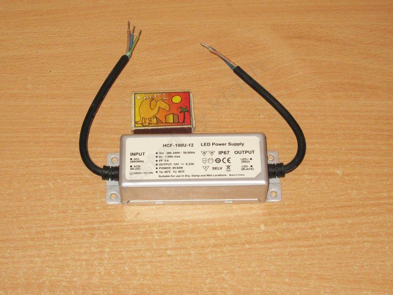
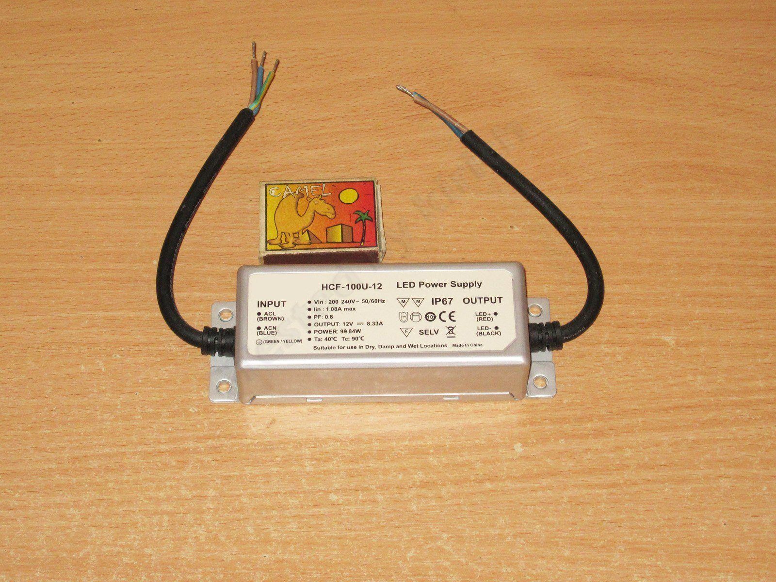
The second power supply: 12 V, 100 W, 8.33 A.
It’s structurally an exact copy of the previous one, just a little larger.
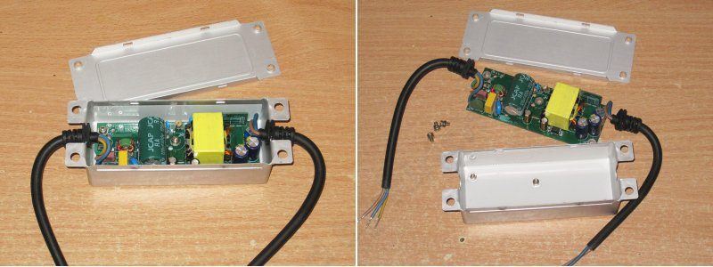
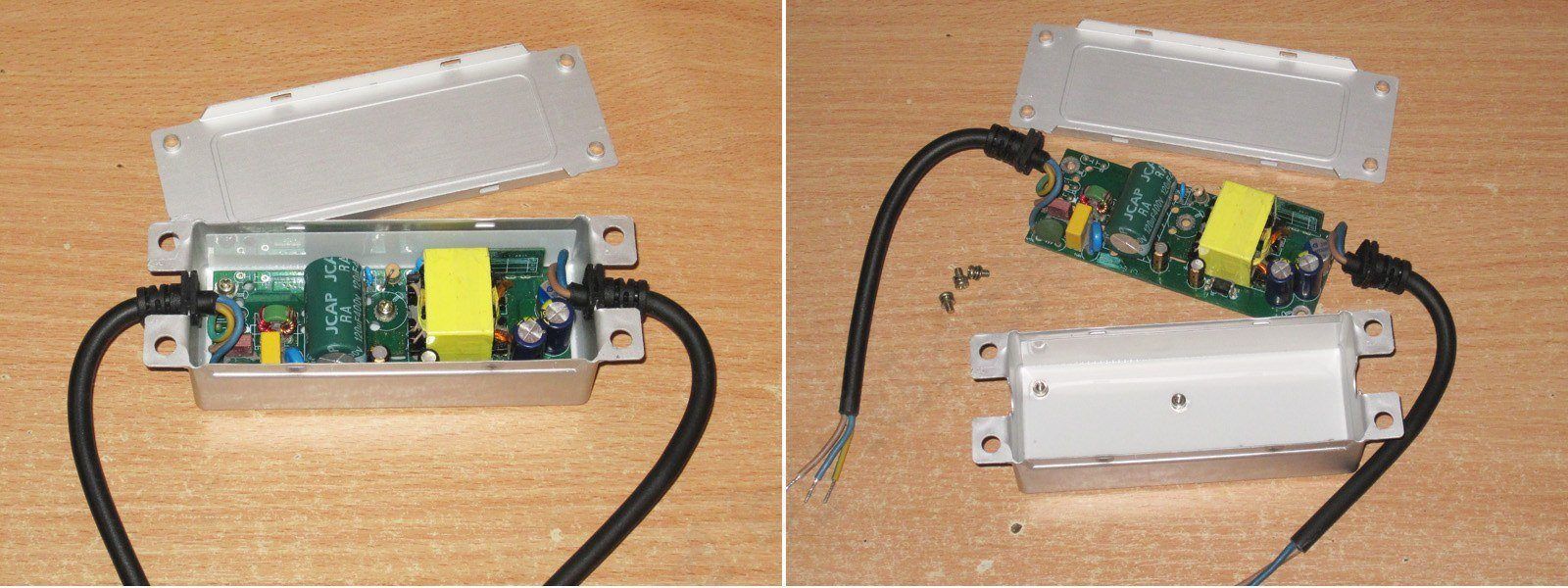
Everything inside is exactly the same, except there are now three screws :)
The board has also been cleaned of potting compound, but the board markings have been sanded off as well. That’s not paranoia anymore; it looks more like this isn’t the power supply manufacturer, but an intermediary.
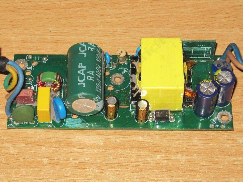
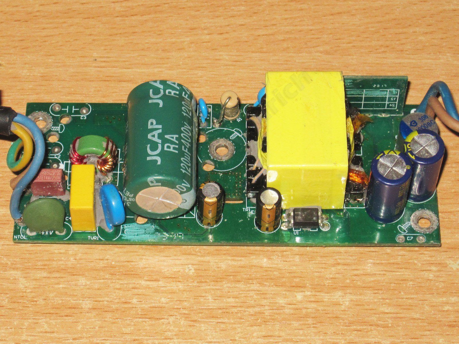
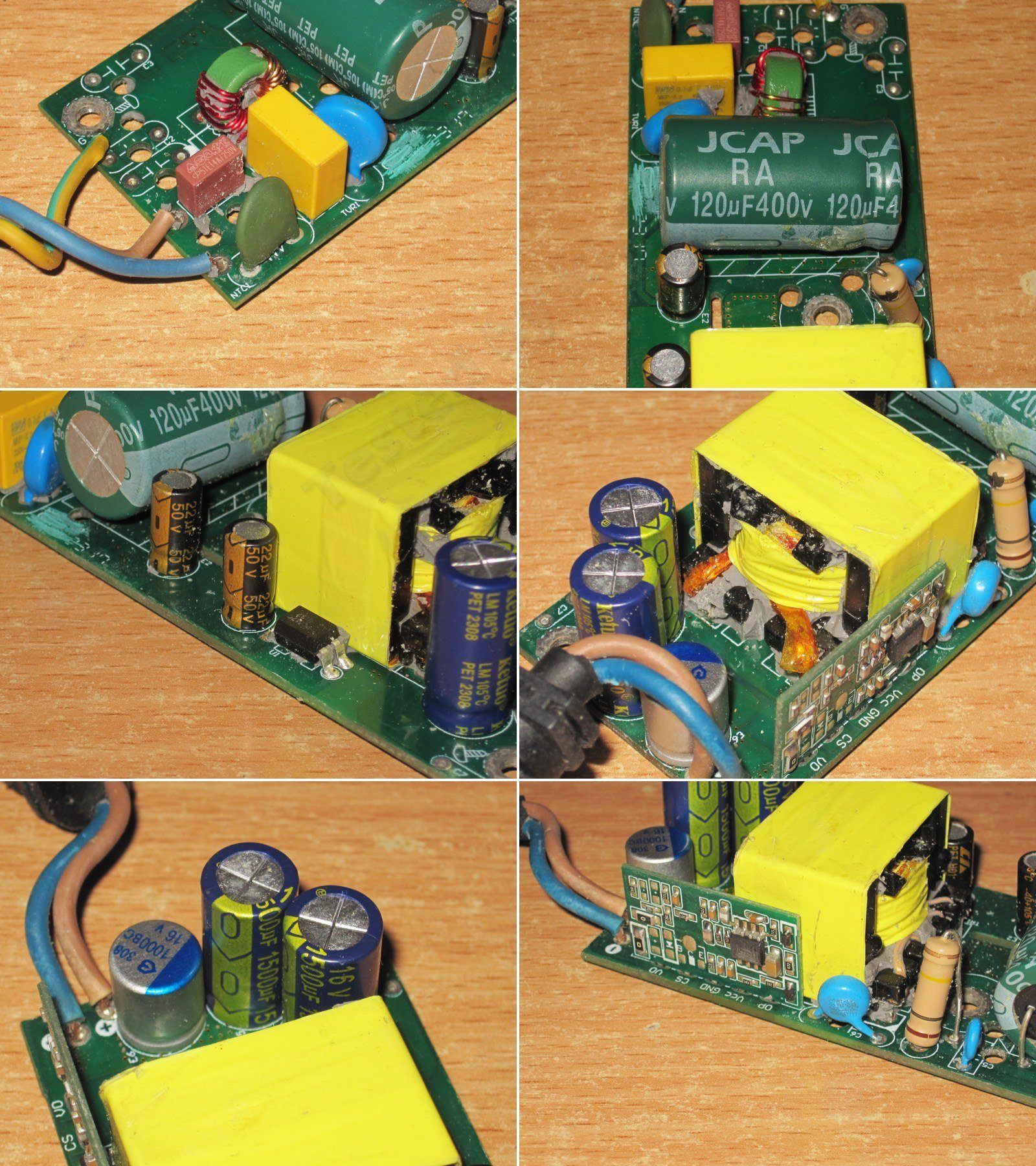
1. The input filter is the same as on the previous unit.
2. The input capacitor is noticeably more substantial this time.
3. An optocoupler, and even a slot beneath it. Interestingly, there are two small capacitors on the high-voltage side here.
4. The transformer winding is also made with Litz wire.
5. On the output, there are two regular 1500 µF capacitors and one 1000 µF polymer capacitor.
6. And, just like before, there’s an additional board installed—in essence, a standardized submodule. A solution that isn't always applicable, but is quite convenient and makes it easy to scale power supplies with less effort.
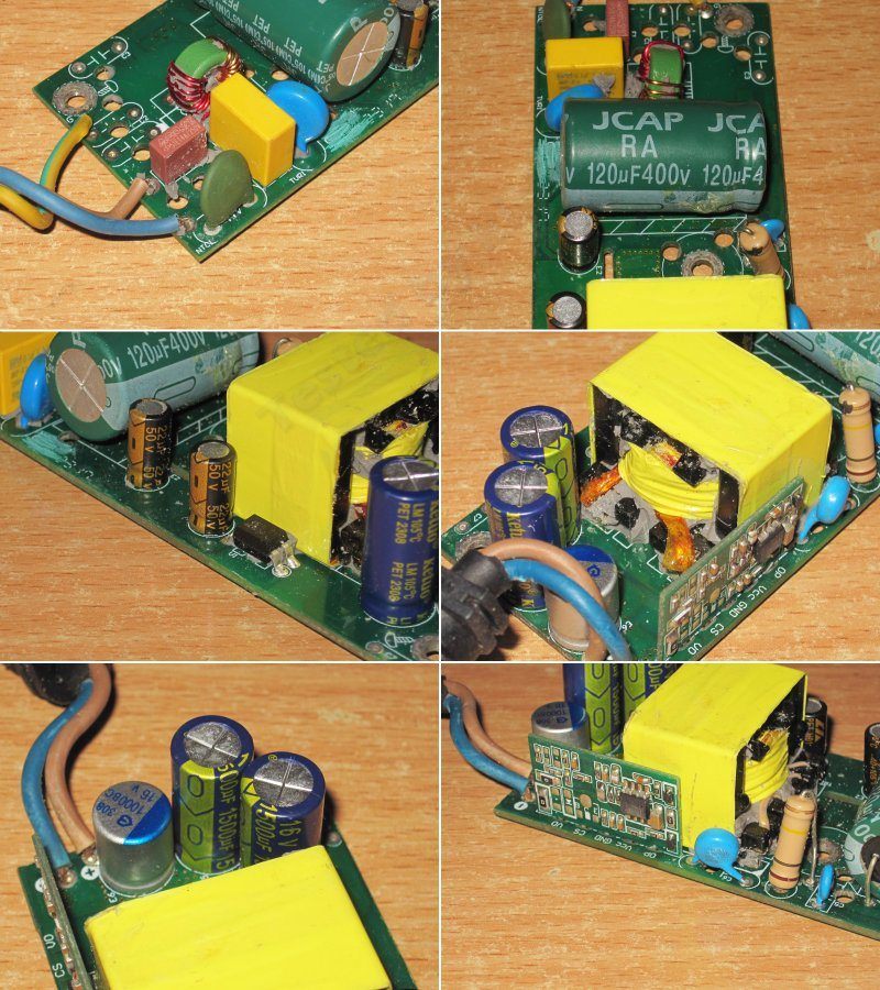
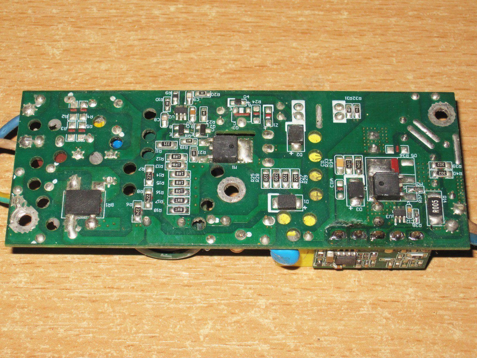
As with the previous one, I have no safety concerns: there are clearances and slots, and even a ground connection.
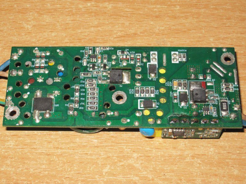
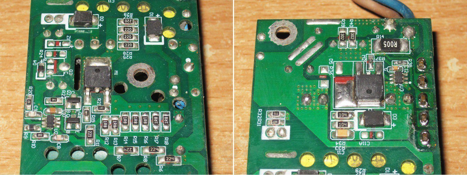
The circuit design here is a bit more complicated, though.
An emitter follower has been added on the primary side to improve control of the high-voltage transistor.
On the secondary side, they used a synchronous rectifier. You can tell from the small chip in a SOT-23-6 package that controls the MOSFET.
The shunt here is 5 mΩ, compared with 10 mΩ in the previous one, but the output current is almost twice as high.
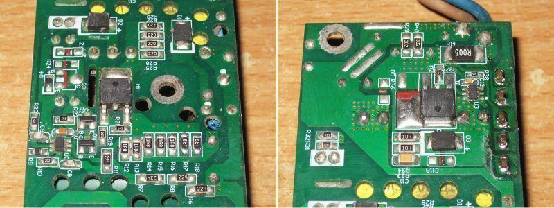
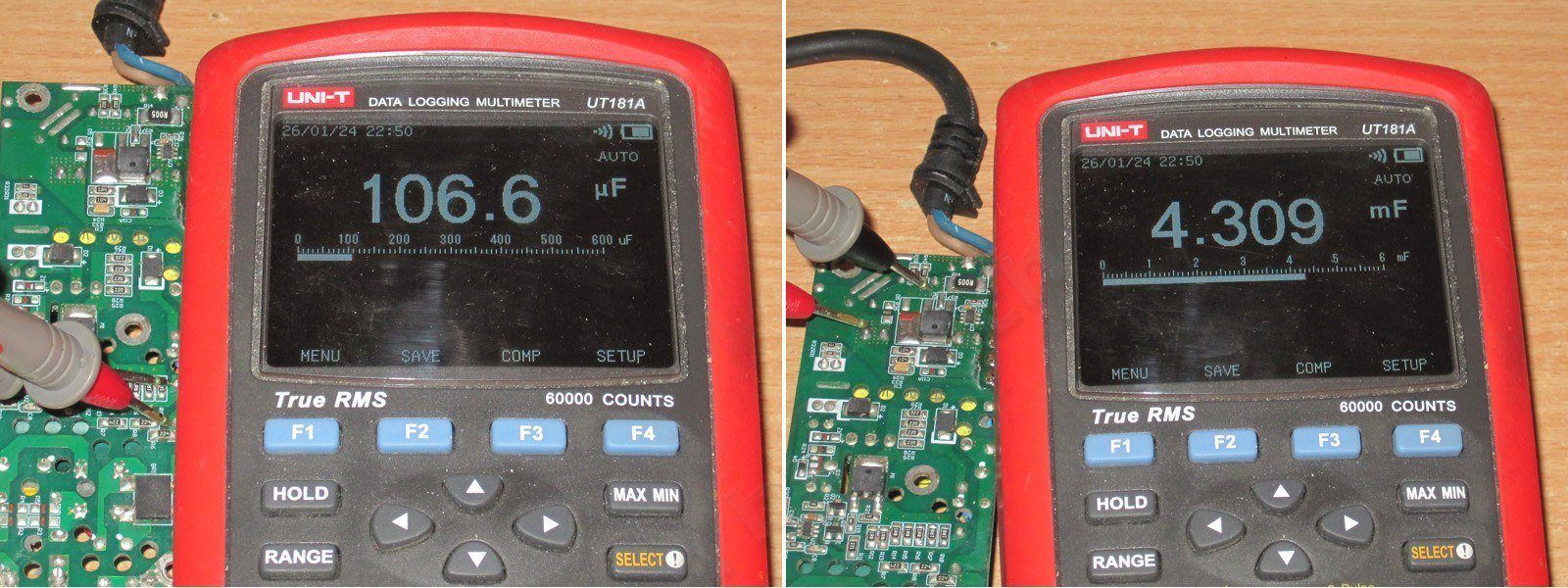
The input capacitor's actual capacitance is 106 µF, which is fine for 100 W of power. The output capacitance is 4300 µF, also fine.
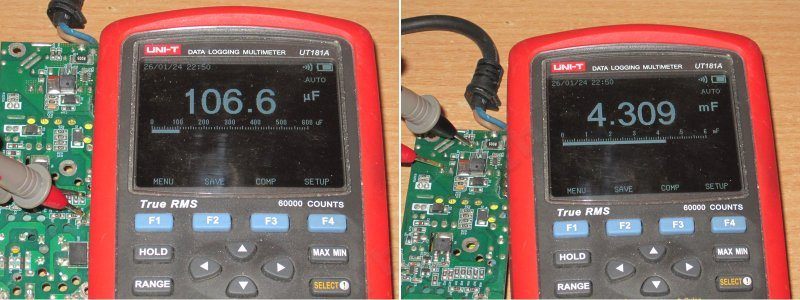
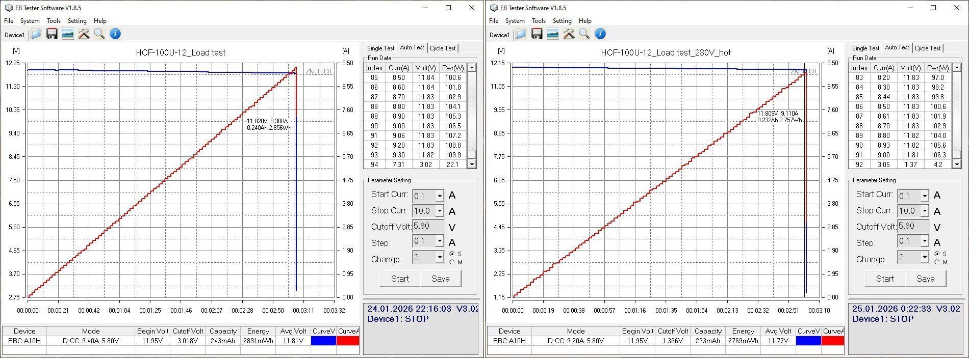
The protection trips at around 9.3 A when cold and 9.1 A when hot, which seems a bit high if the idea is to allow parallel operation. In standalone mode, though, it's perfectly fine.
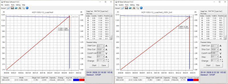
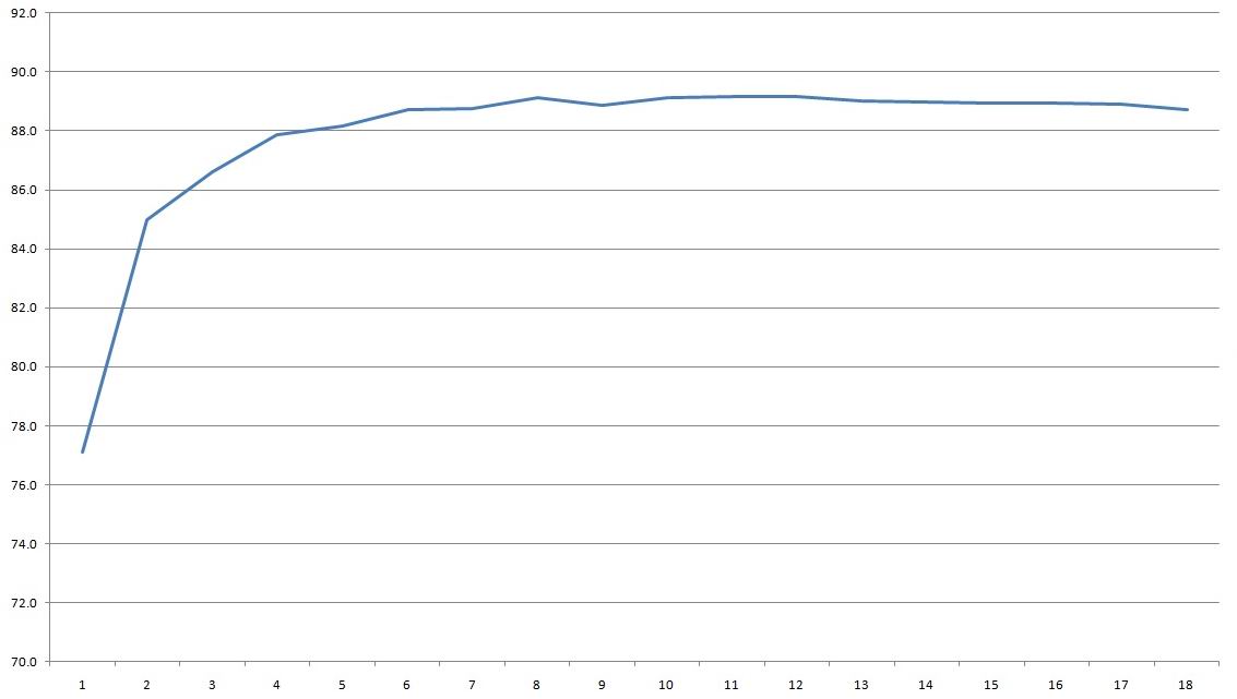
Efficiency is around 89%. Given the synchronous rectifier, that was pretty much expected. It was measured from 0.5 to 9 A in 0.5 A increments.
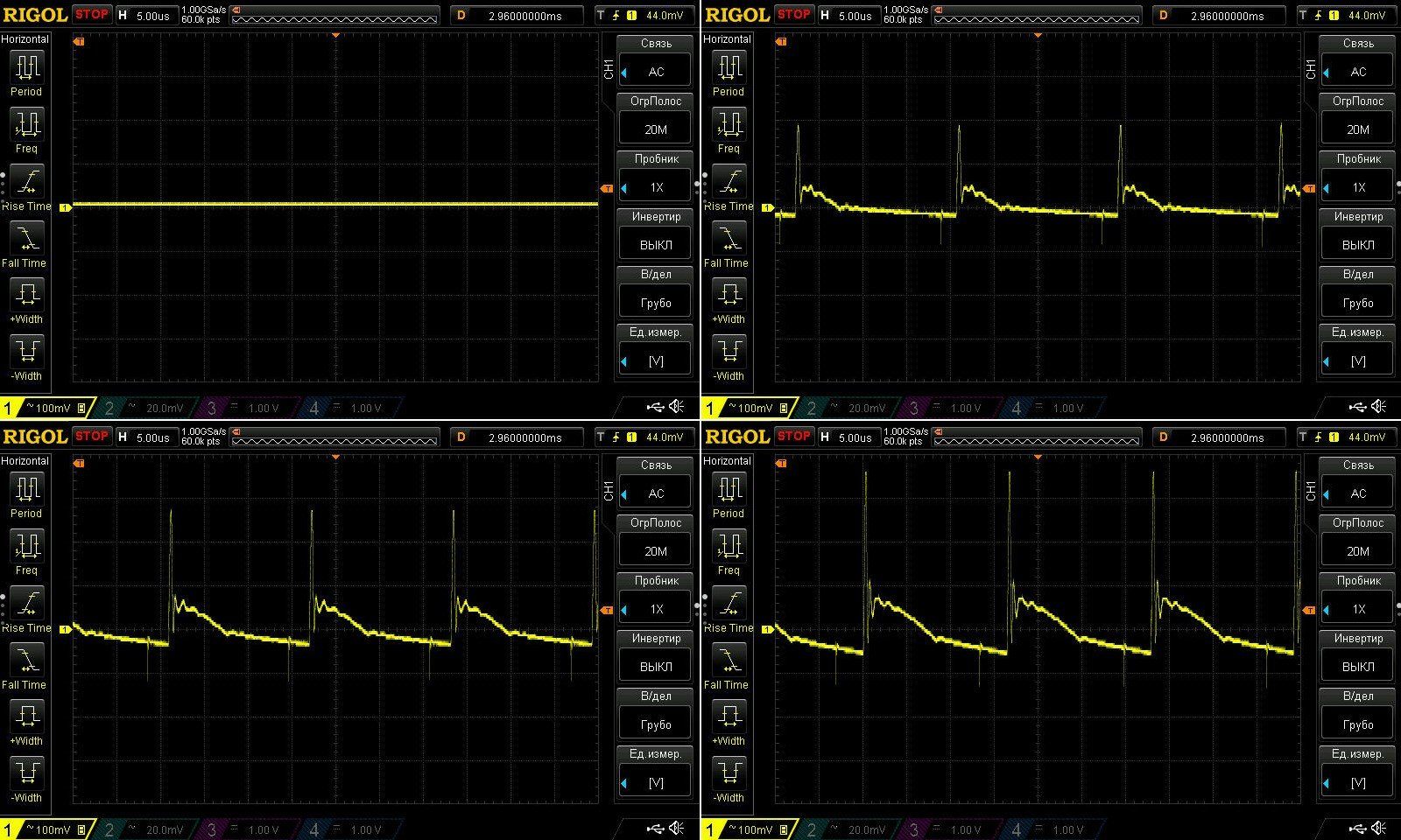
Ripple with no load and at 3, 6, and 9 A.
I wouldn't say 400 mV at maximum current is a lot, though of course less is always better. The main component is noticeably lower; the large peak-to-peak value is due to a short pulse. I think it would be noticeably higher without the polymer capacitor.
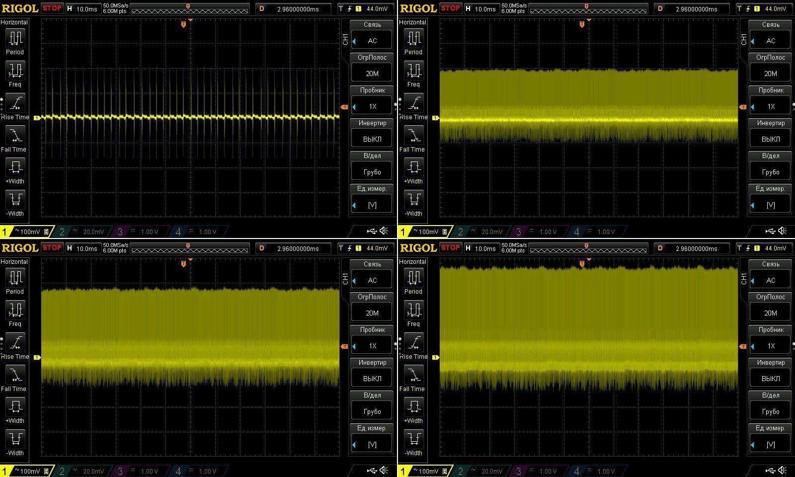
No issues at 100 Hz, but with an input capacitor like this, you'd expect it to perform well.
The test was carried out in four stages, at 2.5, 5, 7.5, and 8.5 A. The voltage regulation under load is good, considering the measurements were taken after the output cable, and the voltage barely depends on temperature.
Temperatures at 5, 7.5, and 8.5 A.
At 5 A: the transistor is at 70 °C, though the snubber diode nearby gets quite hot; the rectifier transistor is at 73 °C, and the transformer at 65 °C. All fine.
At 7.5 A: the transistor is at 94 °C, the rectifier transistor at 109 °C, which is a bit high, and the transformer at 84 °C, which is fine.
At 8.5 A: the high-voltage transistor is at 105 °C, which is a bit high; the rectifier transistor is at 128 °C, which is too high; and the transformer is at 91 °C, which is fine.
So basically, my main concern is the output rectifier transistor; it's running a bit too close to the limit. If you pot it with compound, things will probably improve, and it should even work at the maximum current of 9.1–9.3 A, but it's hard to say how it'll do in hot weather.
By the way, I've been wondering whether ChatGPT could be used for calculations like these.
Third model: 12 V, 150 W, or 12.5 A
And once again, it's basically a larger version of the previous model.
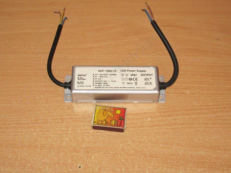
150 W is a threshold power level: often too much for a flyback converter, but too little for other topologies, so I'm always curious to see what the manufacturer chose.
Here we have a single-switch flyback converter. In my opinion, 150 W is already pushing this topology close to its limits.
When I took the board out of the case, I also noticed a pair of thermal pads, several millimeters thick. They're installed in an unusual way, transferring heat through the plastic insulation.
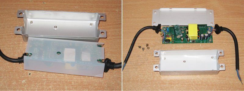
The board looks very much like the previous model. It even has the same two small capacitors, though there are more on the output side.
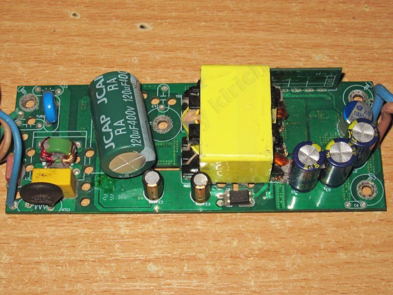
The filter, varistor, input capacitor, and the pair of small capacitors mentioned earlier—no, really, it's a copy of the previous power supply.
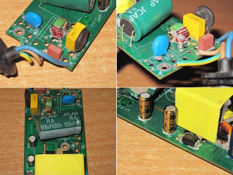
The submodule layout, Y capacitor, and litz-wire transformer winding—in essence, the manufacturer just scaled up the design a little and added one 1500 µF output capacitor. It was 2 × 1500 + 1000 µF; now it's 3 × 1500 + 1000 µF.
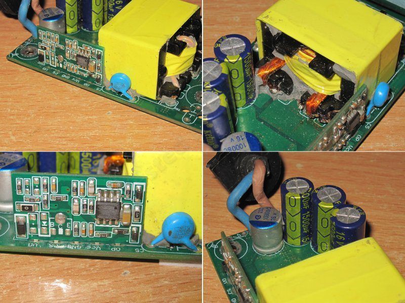
I even put them side by side in the end, because when you look at them separately, they really do seem like the same power supply.
But they're not. First, there are clearly some differences; second, the board itself is larger, though there's still a lot in common. In principle, this is a perfectly reasonable way to scale things up.
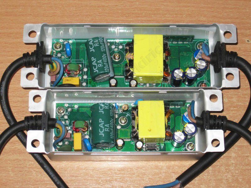
They decided not to replace the bridge rectifier, just added a second one in parallel—and also removed the markings from the bridge rectifier. Good grief, I'm shocked.... Apparently they gave the units to a student and told him, “Dig out the potting compound and erase the markings on everything you can see.” At least he didn't erase the markings on the resistors :))))
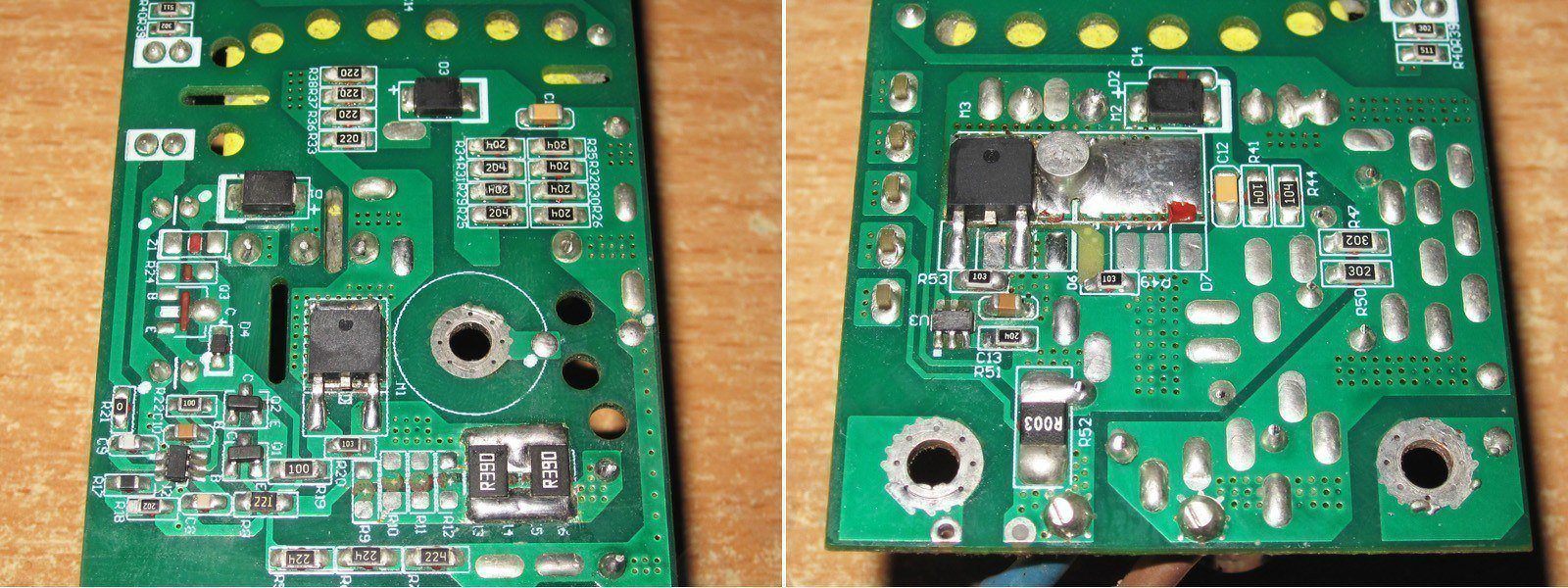
There are two thermal pads. The one on the right is obvious: that's clearly the output rectifier. But the one on the left isn't on a transistor, which would have been the usual arrangement.
I have no complaints about the board itself; overall, everything makes sense, and it was clearly laid out by someone with plenty of experience.
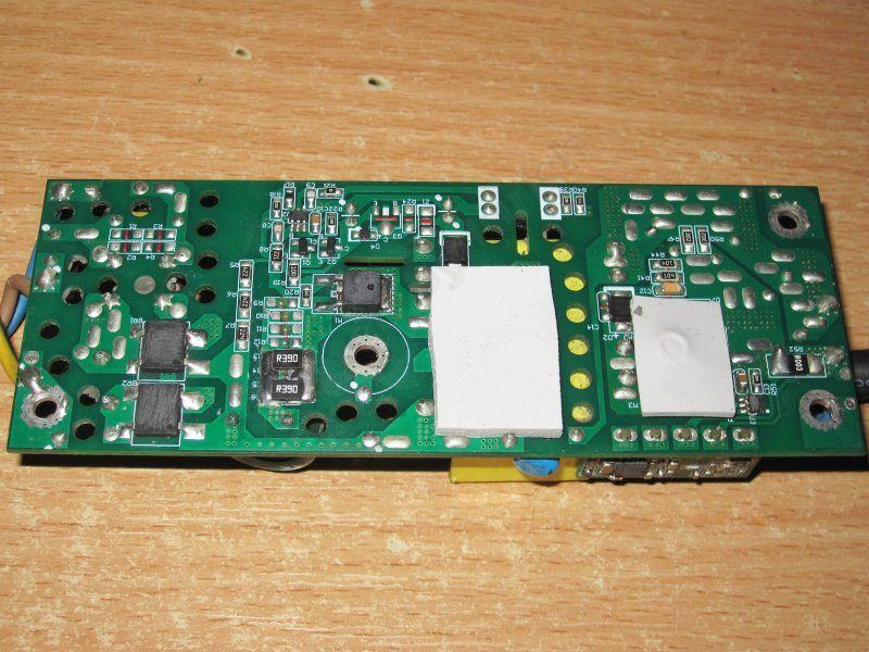
1. So, the pad was hiding a snubber. And yes, this is all correct: the more power you try to draw from a flyback converter, the harder the snubber has to work. So the designer made the right call in their own way by transferring its heat to the case. Doing it through plastic insulation, though... not ideal. Maybe they planned to add a window there.
2. The output uses a synchronous rectifier, but I somehow expected to see two transistors. There are even two footprints for them, so I suspect that was the original plan, but then an “optimizer” got involved. Actually, no—the space on the right is for a diode, not a transistor. Judging by the copper pours, you can fit either one transistor or two diodes, so maybe there was no “optimizer” involved after all.
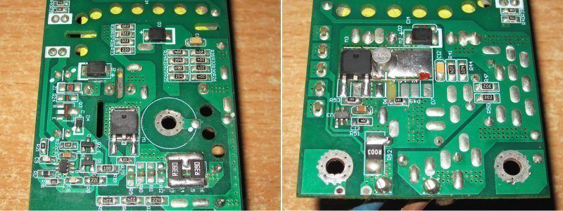
The output current-sense resistor is 3 mΩ. If we assume the 60 W version had a 10 mΩ resistor, the expected current here is about three times higher.
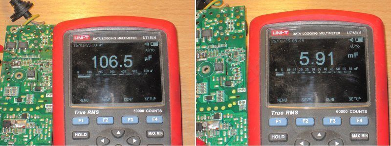
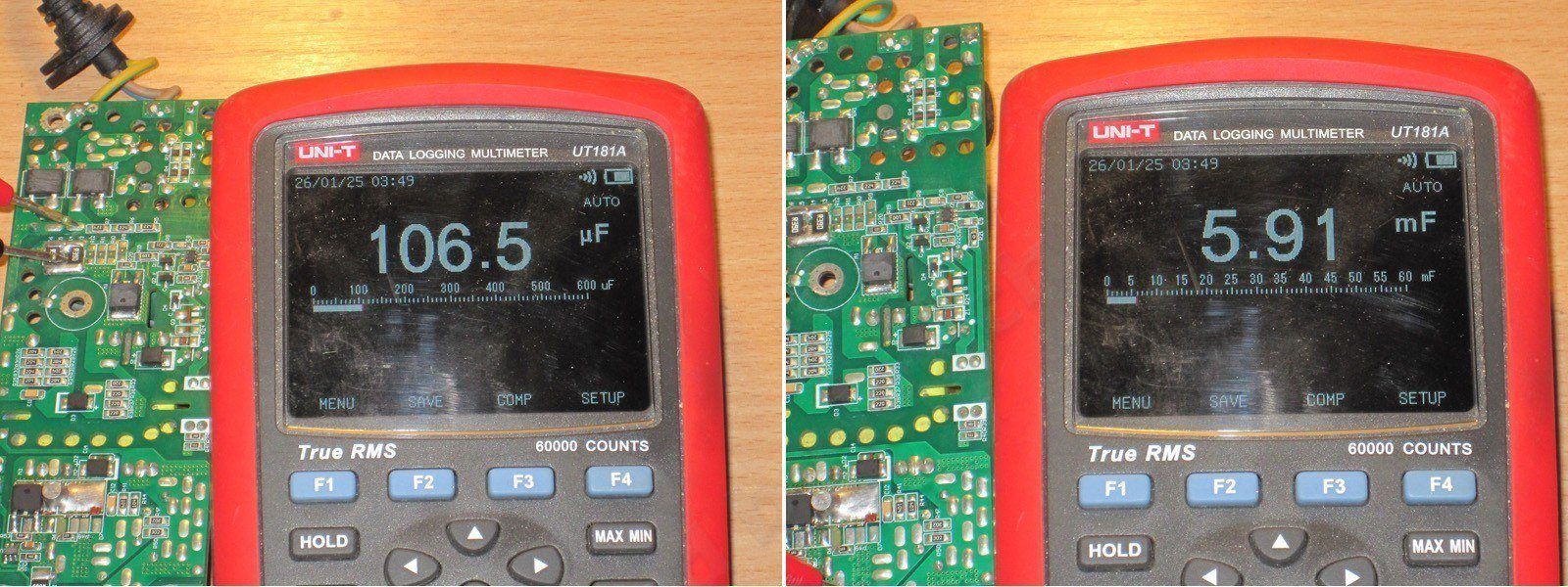
The input capacitor is the same as in the 100 W version. That was fine there, but it's a bit undersized here.
The output has almost 6000 µF, which is fine in principle.
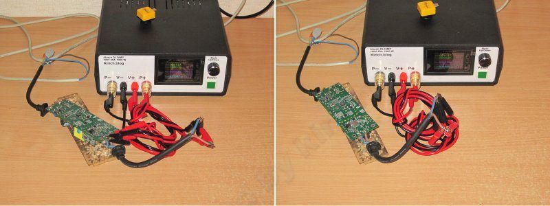
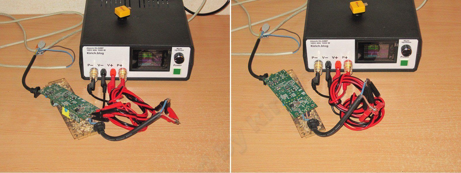
For obvious reasons, I used a different load this time. By the way, it's already been sent off to our military, so I'll have to build a new batch.
I used two connection setups. Efficiency was measured with a four-wire connection, as was the first test of the protection threshold. The long-duration tests also used four wires, but the load was connected to the output wires rather than directly to the board. The thing is, you have to move the board around during a long test, and I was worried something might short out and interrupt the test.
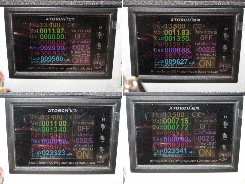
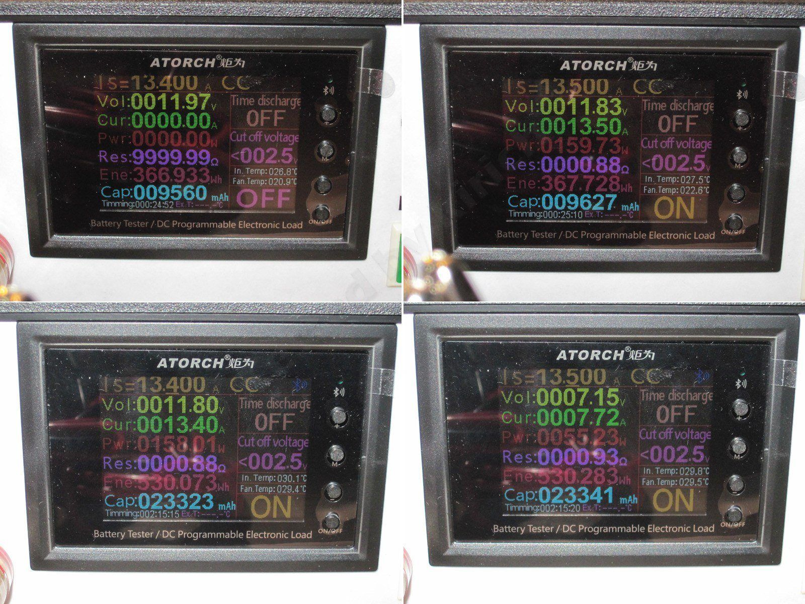
The protection trips at around 13.5 A and is practically unaffected by temperature. The top image shows the power supply cold, the bottom one hot; I even happened to catch the moment it shut down.
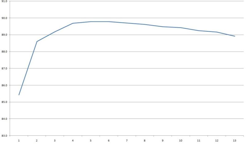
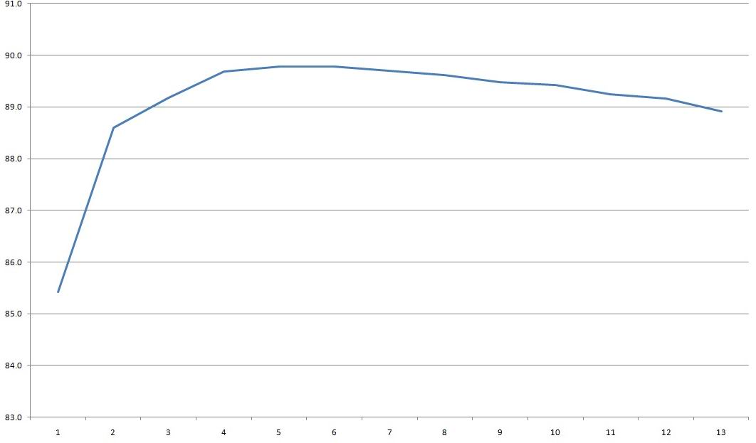
Efficiency was measured from 1 to 13 A in 1 A increments, and came out to about the same 89%. But you can see that efficiency drops at higher currents, which in my view is partly due to overloading the output rectifier. In other words, one transistor simply can't handle it, and its losses approach those of an ordinary Schottky diode.
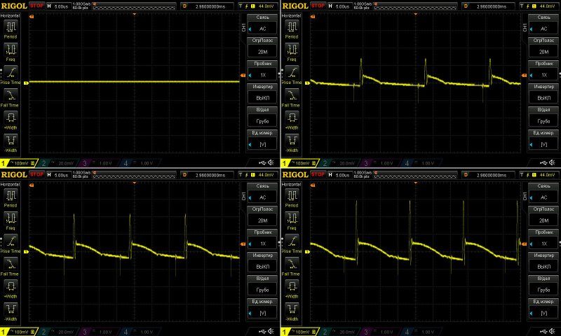
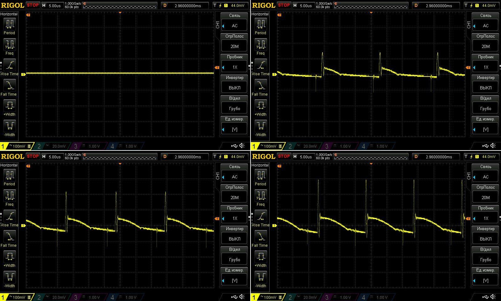
The high-frequency ripple is about the same as on the 100 W version: around 400 mV peak-to-peak and about 120 mV for the main component. Unfortunately, power supplies with this kind of topology usually have noticeable ripple; it's inherent to the topology itself. But I should point out that for a flyback converter, and without an output filter, it still looks relatively good—which means the board layout is sound.
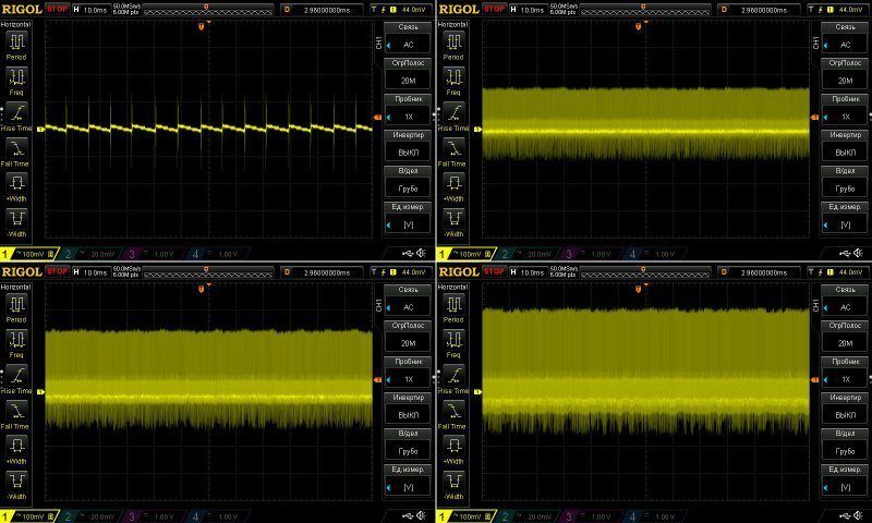
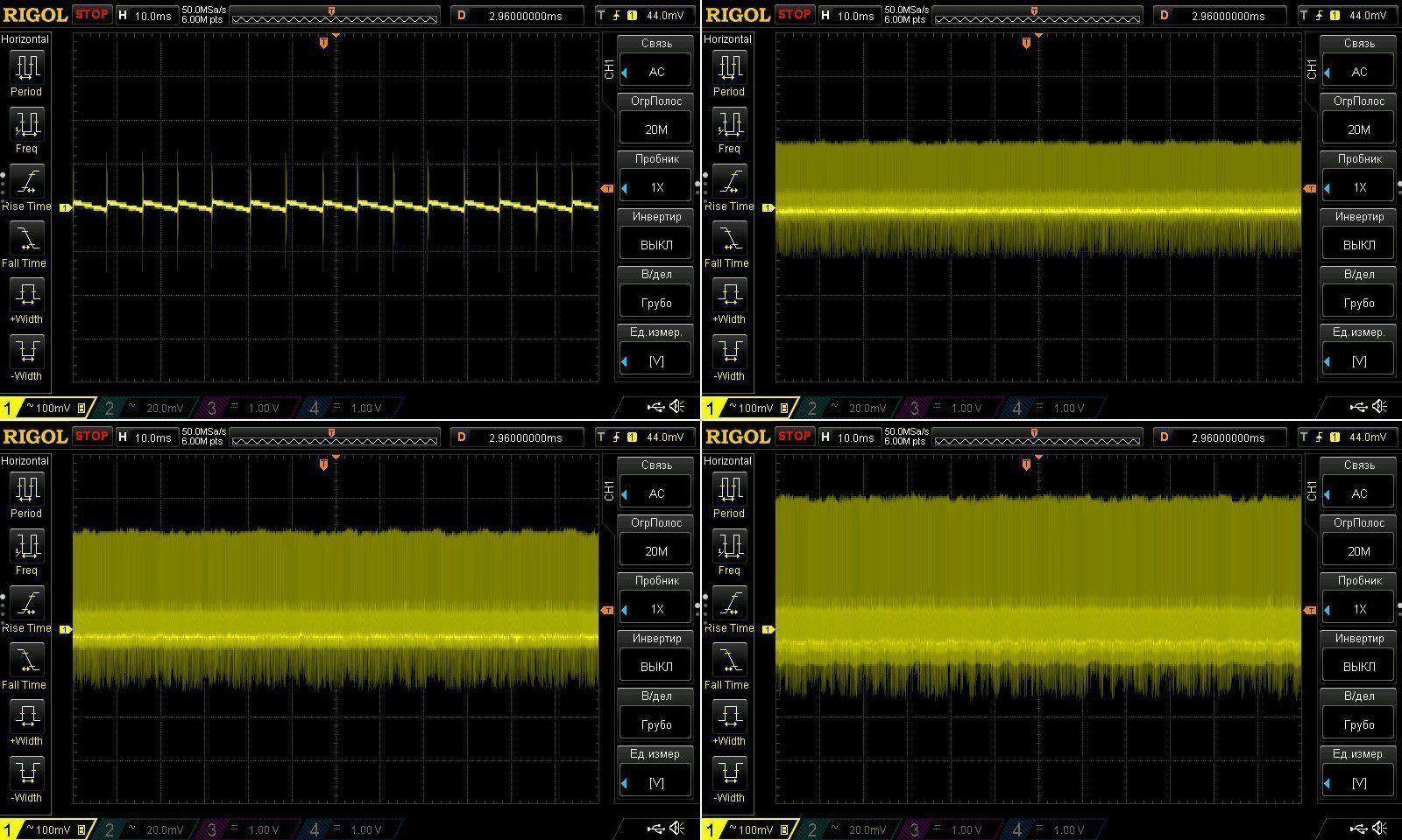
At 100 Hz, the results are about the same as on the 100 W version, with no issues.
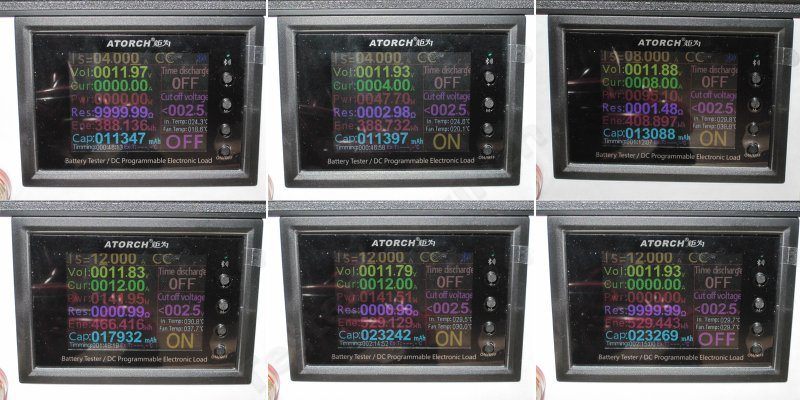
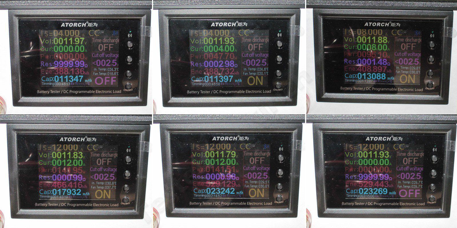
The load test was run at 4, 8, and 12 A, for a total of about 1.5 hours.
The photos show the voltage with no load, at 4 A, 8 A, and 12 A at the start of each stage, then at 12 A at the end, and finally the voltage after removing the load.
You can see a slight change in voltage with load, about 40 mV. By the way, moving the feedback circuitry onto a submodule helps keep the output voltage stable as the temperature changes, since the feedback circuitry itself is farther from the heat source.
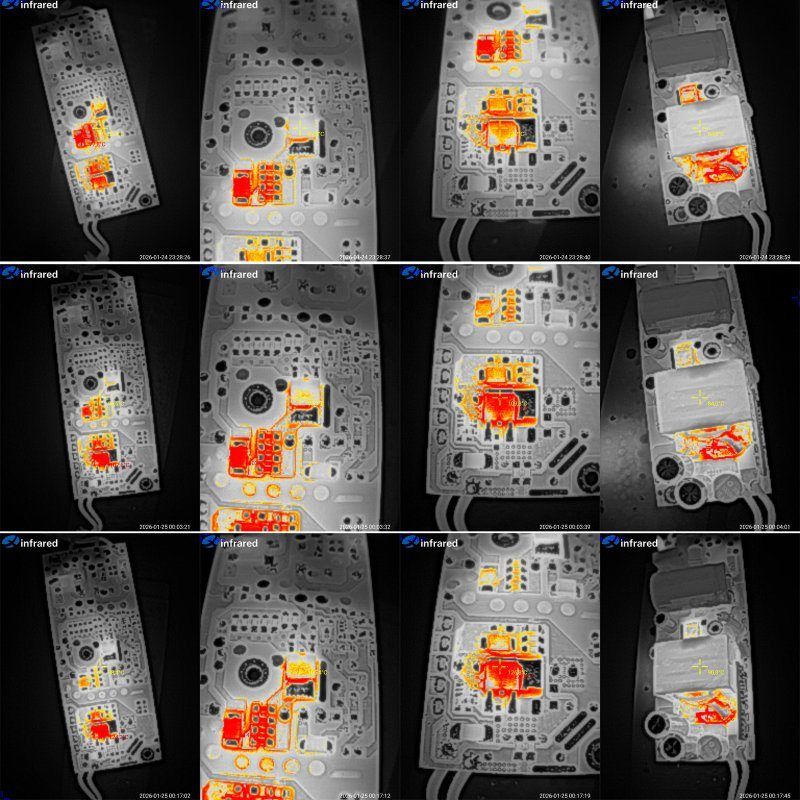
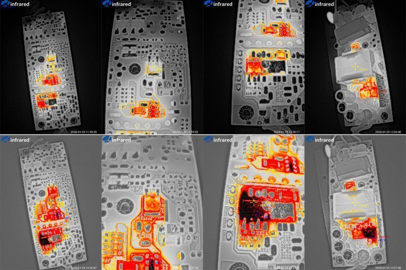
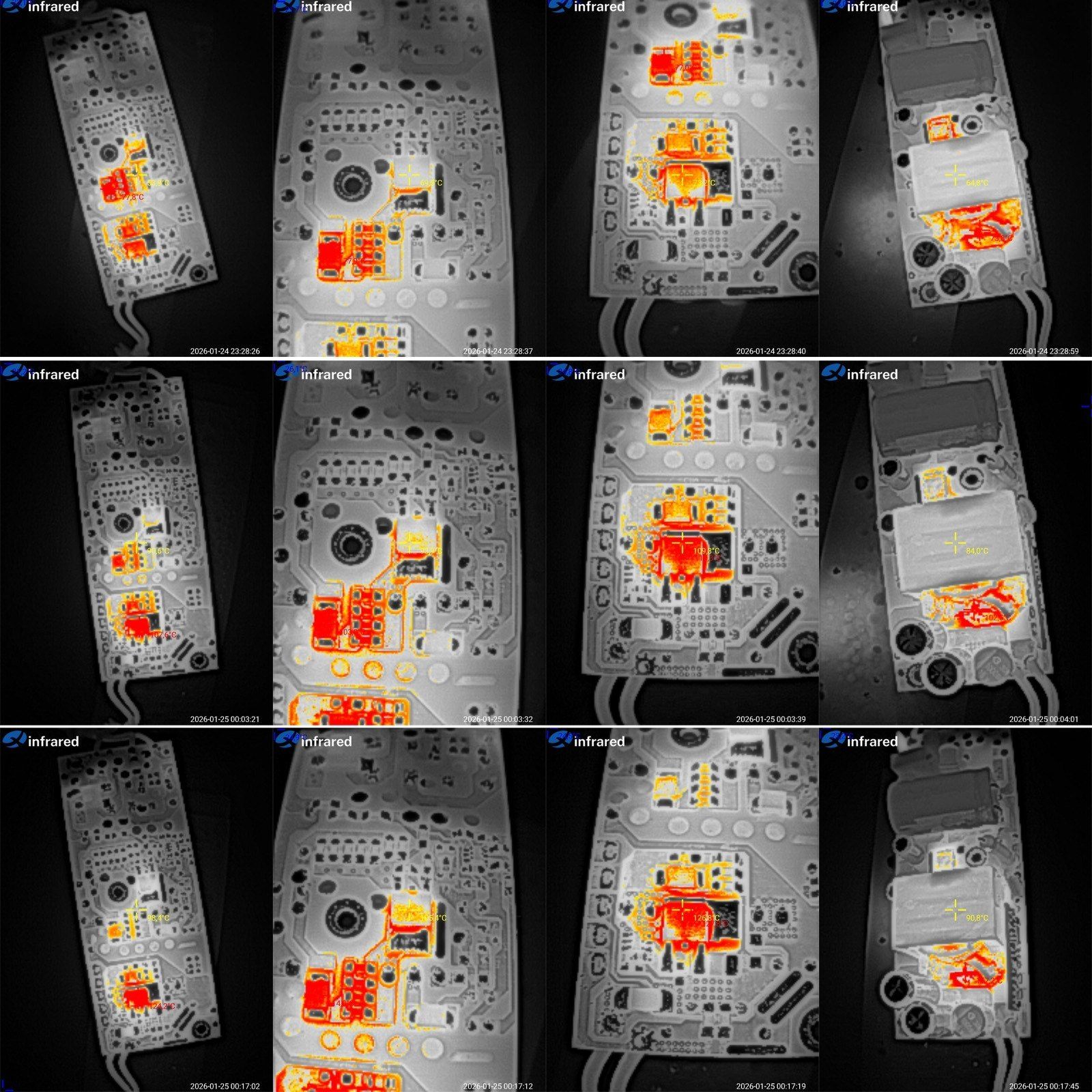
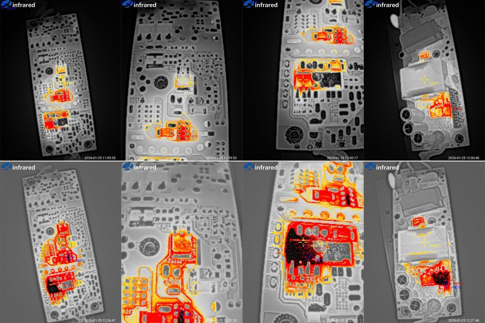
Temperatures at load currents of 8 and 12 A.
8 A — you can see the hot spot on the snubber. The transistor is at 82°C, which is fine; the rectifier transistor is at 93°C, also fine; and the transformer is at 73°C, which is perfectly acceptable too.
12 A — the snubber temperature is off the scale, above 130°C; that's a lot. The transistor is at 125°C, also too high. The rectifier transistor has likewise exceeded the thermal camera's 130°C limit, and the transformer is at 107°C. That's rather high.
It's clear that the scaling wasn't done very well: the snubber and rectifier transistor are obviously overheating, and the high-voltage transistor is getting quite hot too. The results should improve once the unit is potted and some of the snubber's heat is transferred to the case. Still, in my view, they could at least have added another output transistor. That would have made a noticeable difference by spreading the heat across two packages and reducing the voltage drop. The snubber would dissipate heat better if there were a cutout for a thermal pad, but the transformer is fine as it is; the potting helps it quite a bit.
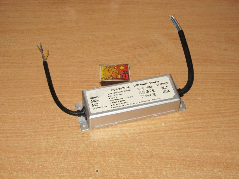
And now the larger 12 V, 200 W model, rated at 16.86 A.
Visually, it's just a scaled-up version of the previous three.
The layout is similar, but the differences are much more noticeable here—and, by the way, there are no thermal pads.
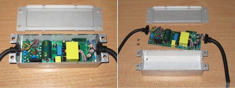
It's clear that this uses a classic LLC topology: an inductor, a transformer, and a capacitor.
As with the previous models, the board layout is fairly spacious, which is good.
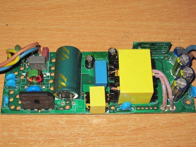
1. The input filter is a little better than on the previous models: several Y capacitors have been added, and a more powerful bridge rectifier is used. The input capacitor, though, is the same as in the 100 W and 150 W versions, which is a bit small... But given that the specified input range starts at 200 V, it should be adequate, just barely.
2. The classic LLC topology itself.
3. Interestingly, in addition to the two capacitors on the primary side, there's another small one on the secondary side.
4. Interwinding Y capacitor.
5. On the output, there are three standard 1500 µF capacitors and one 1000 µF polymer capacitor, which is perfectly adequate for this topology.
6. There's an additional capacitor between the output and the case.
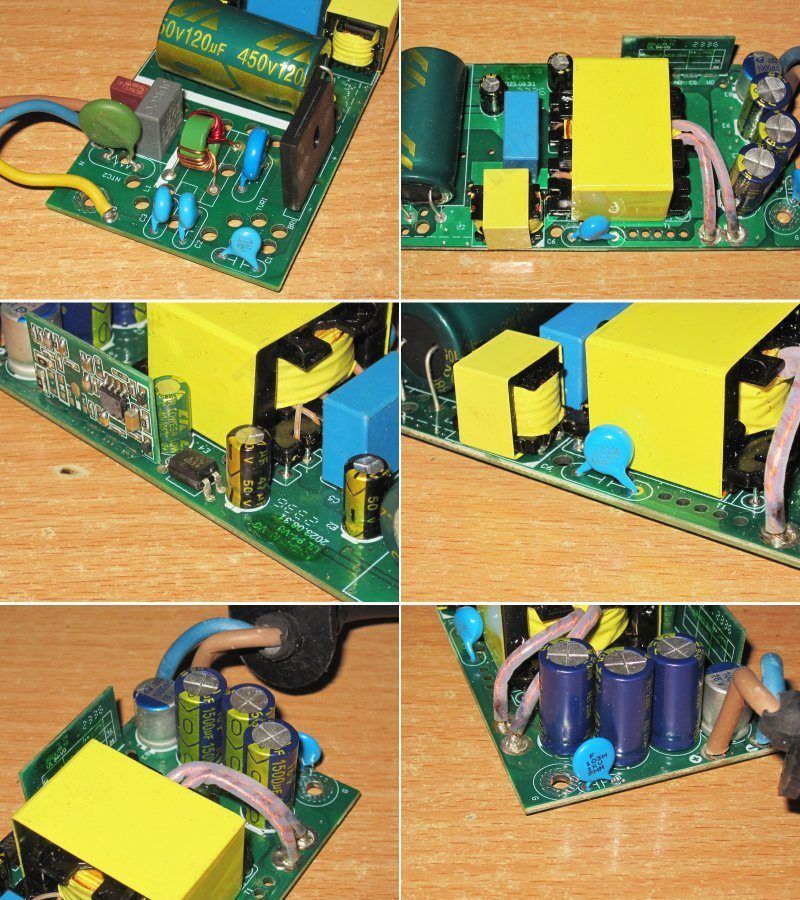
No safety-related issues with the PCB layout. You almost want to say, “See, they can do it when they want to...”
Oh, and I almost forgot: this is the only one of the four power supplies that wasn't cleaned of potting compound—it arrived clean.
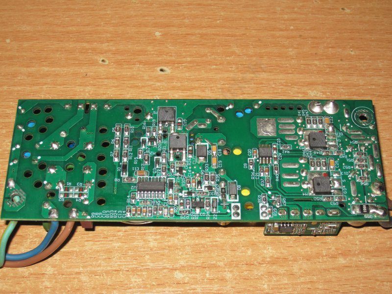
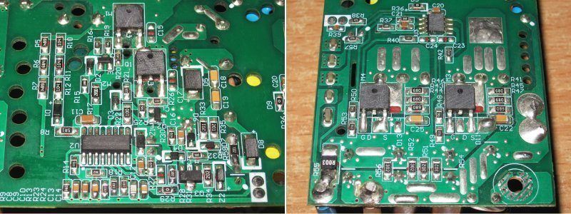
1. All the component markings have also been removed from the input section, but I think the controller is something like a TEA2016, since there aren't that many LLC controllers. Interestingly, I couldn't find a current-sense resistor on the primary side.
2. On the output side, there's a 3 mΩ shunt and two synchronous rectifier transistors. I wonder if they could get it down to just one? :)
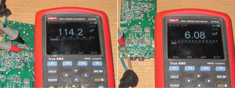
Interestingly, the input capacitors in the 100 W and 150 W models had an actual capacitance of 106 µF, while this one, which looks identical, measures 114 µF.
About 6000 µF on the output, no complaints there.
The protection trips at around 18–18.1 A, regardless of temperature.
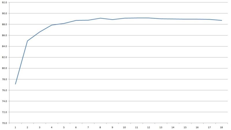
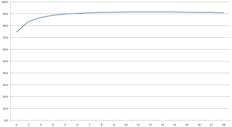
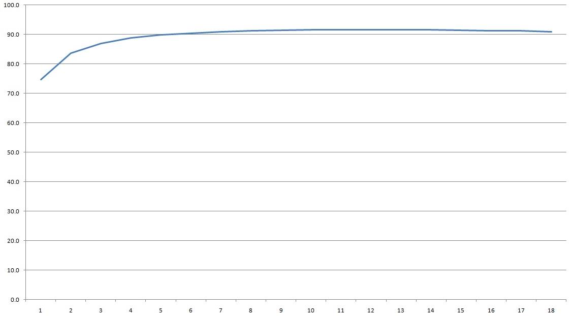
I measured efficiency from 1 to 18 A in 1 A increments. Across almost the entire range, I got around 90–91%, and the efficiency curve is practically flat.
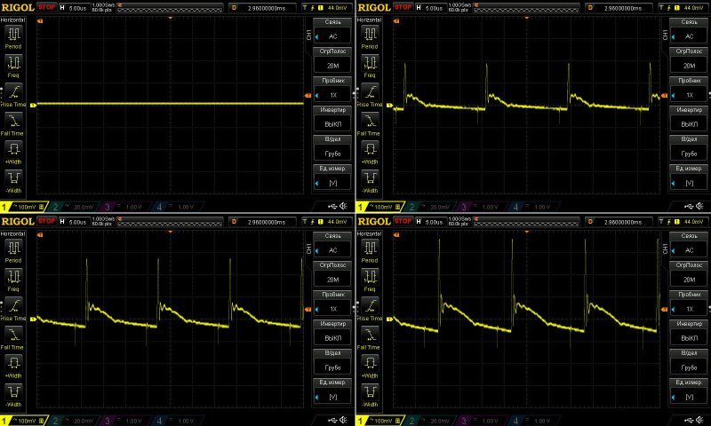
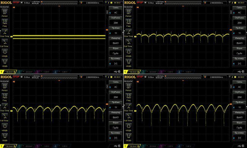
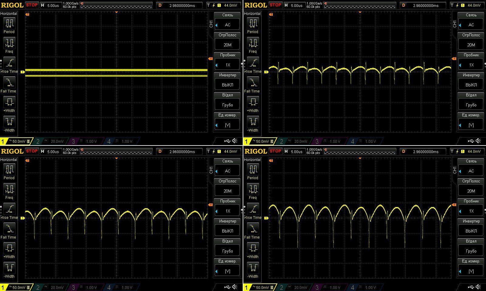
Ripple at no load and at currents of 6, 12, and 18 A.
The high-frequency ripple looks great: even the full swing is only 150 mV, and most of it is within 50 mV. But as I often point out, that's mostly down to the topology; the same goes for power supplies using a half-bridge topology.
The odd no-load waveform was an accidental result, most likely caused by the “green” mode.
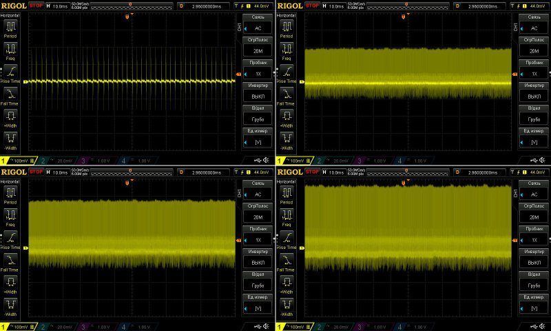
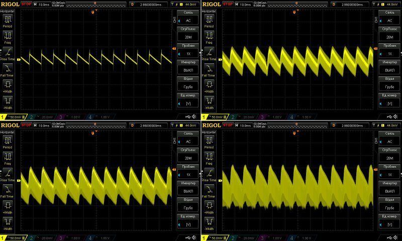
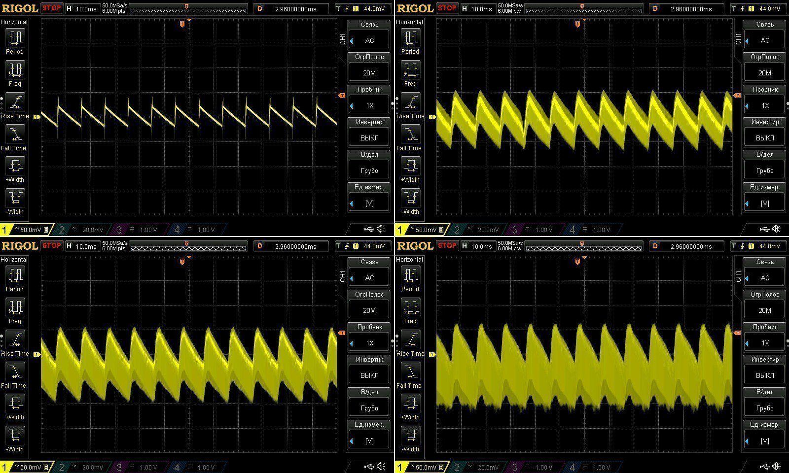
At low frequencies, though, we can see clear 100 Hz ripple. It's not critical for most loads, but this power supply isn't suitable for powering audio equipment.
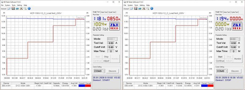
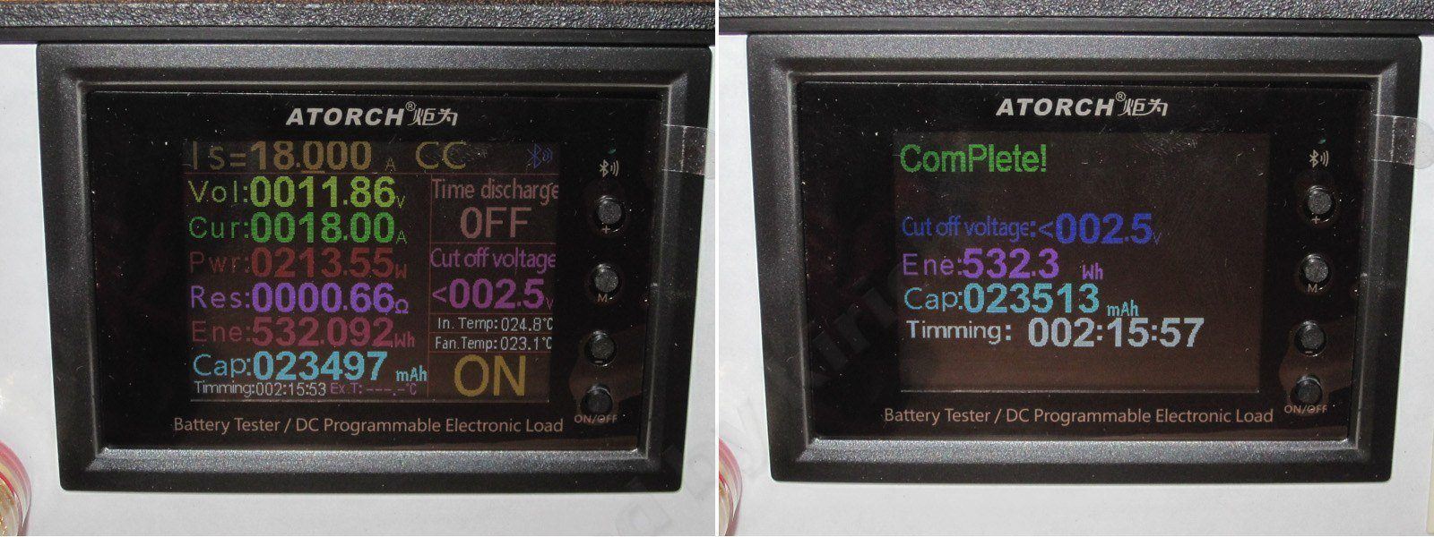
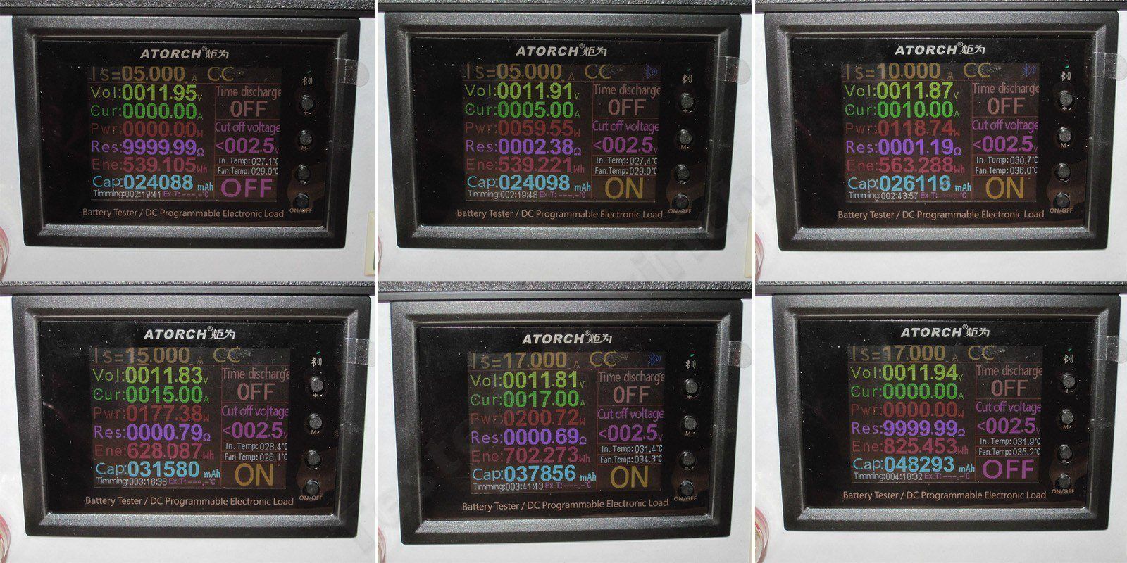
The load test was run at 5, 10, and 15 A. Since the power supply performed quite well, I then raised the current to 17 A, drawing over 200 W (accounting for the voltage drop and cable losses, that's 200 W at the load).
The output current probably has very little dependence on the load, since what we're seeing here also includes the voltage drop in the output cable. There's practically no temperature dependence: it was 11.95 V and became 11.94 V.
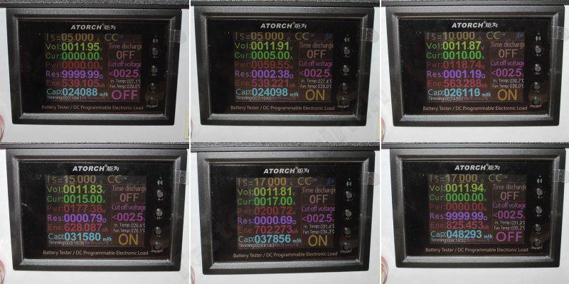
And, of course, the results of the load test. The test lasted about two hours in total, so the power supply had plenty of time to warm up.
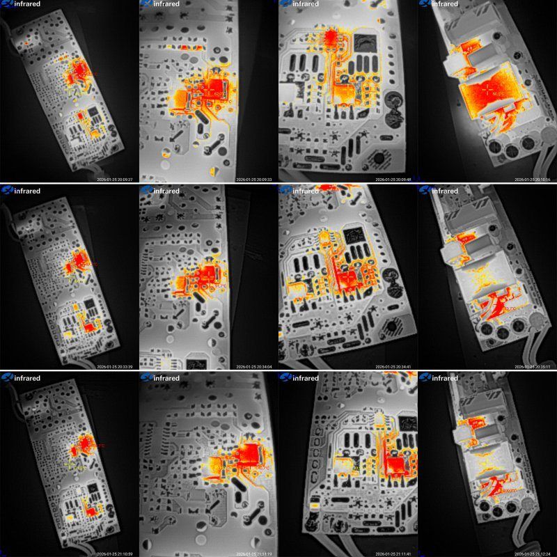
Results at 10, 15, and 17 A:
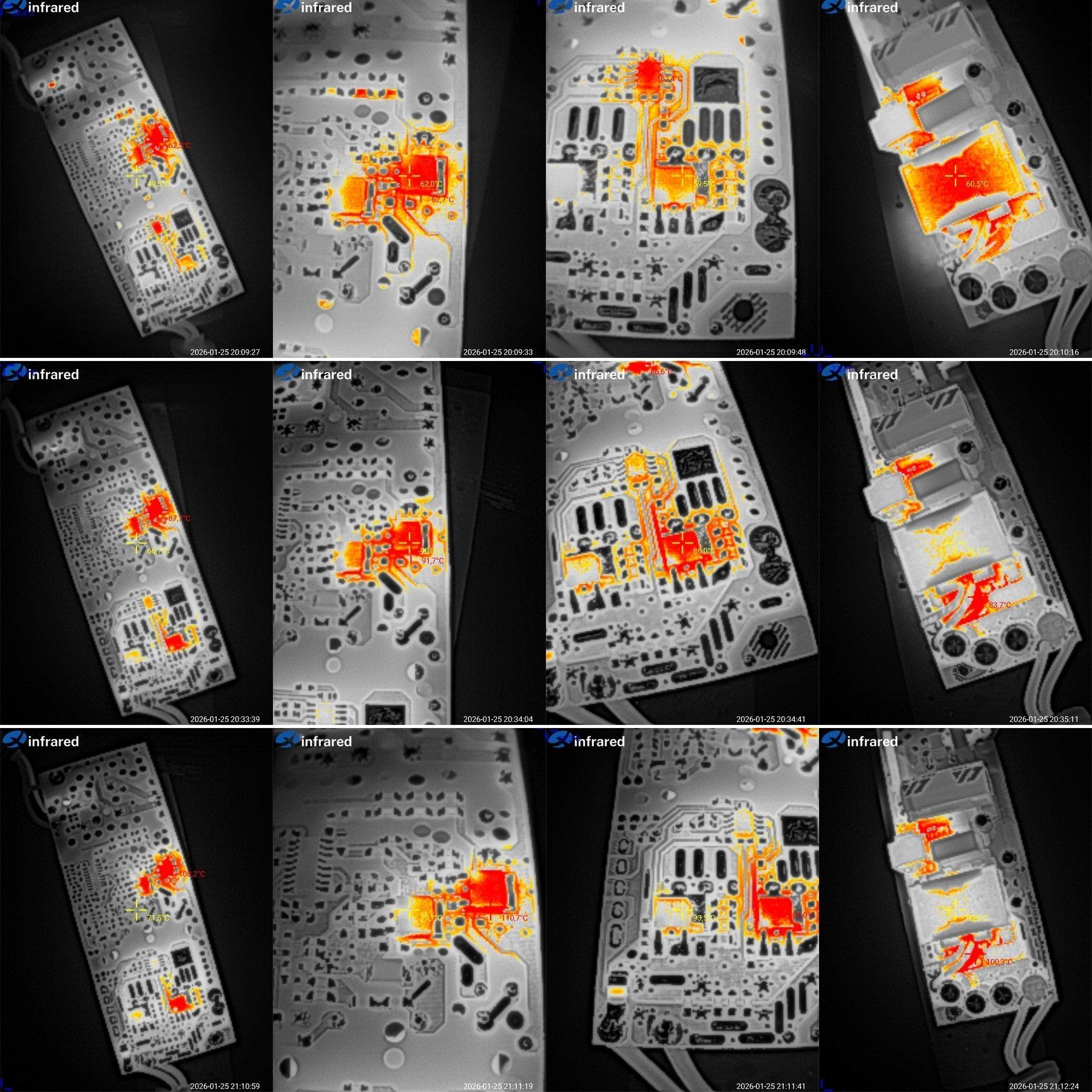
10 A — transistors at 63 °C, rectifier at 60 °C. The rectifier controller actually ran hotter, at 62 °C. The transformer was at 60 °C. No complaints at all.
15 A — transistors at around 92 °C, which is fine; rectifier at 86 °C, good; transformer at 76 °C, excellent.
17 A — transistors at 100 and 110 °C, right on the limit, with the outer one running hotter. The rectifier transistors were at 94 and 105 °C, with the right one hotter; the transformer was at 90 °C, which is good.
As for the temperatures, I can say that, given the lack of heatsinks, the results are actually quite good. This is the power supply I was referring to in my review of the 240 W model in a recent post. That is, There’s a 240 W unit with large heatsinks, and I wouldn’t say it runs much cooler than this 200 W model, which uses polygon-shaped heatsinks on the circuit board.
I think it would work even better if you filled it with potting compound to spread the heat and transfer it to the case. All in all, I think the results are pretty good.
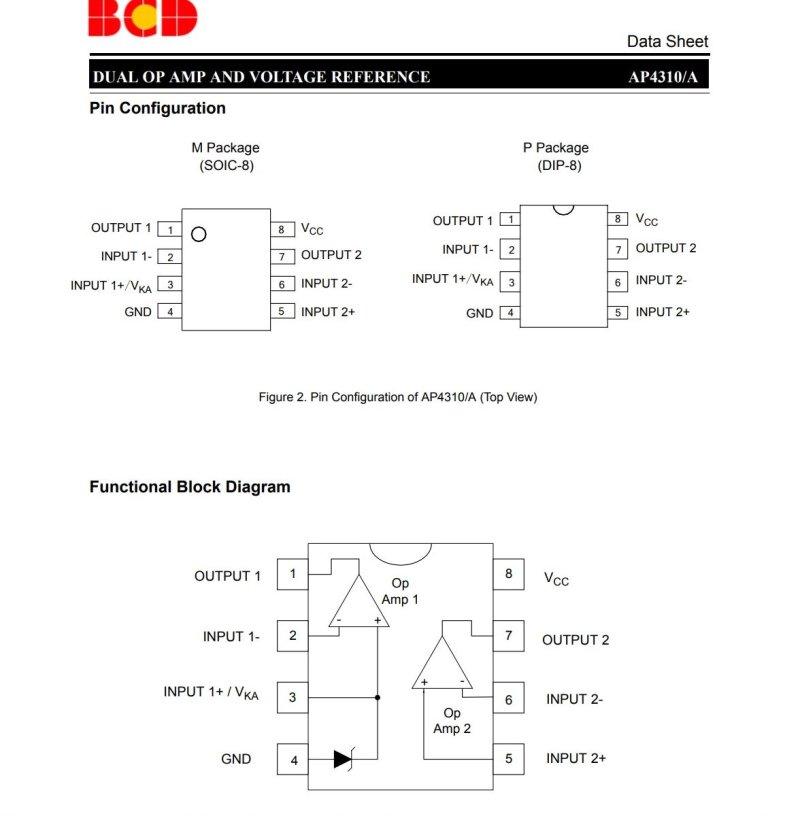
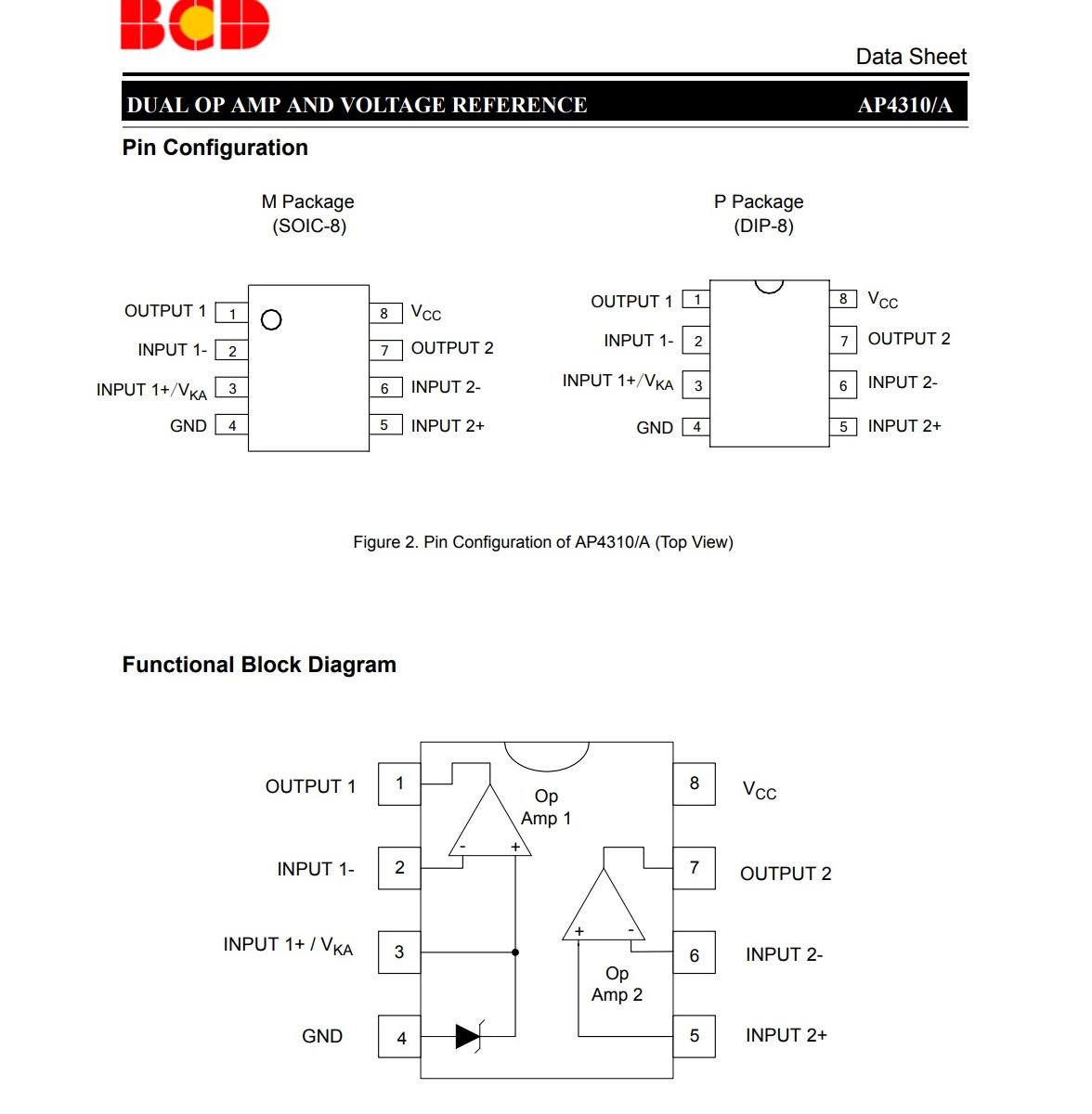
Later, I decided to find out what chip was on the submodule. As it turned out, it really is the familiar AP4310, which means there’s a full-fledged CC/CV mode here.
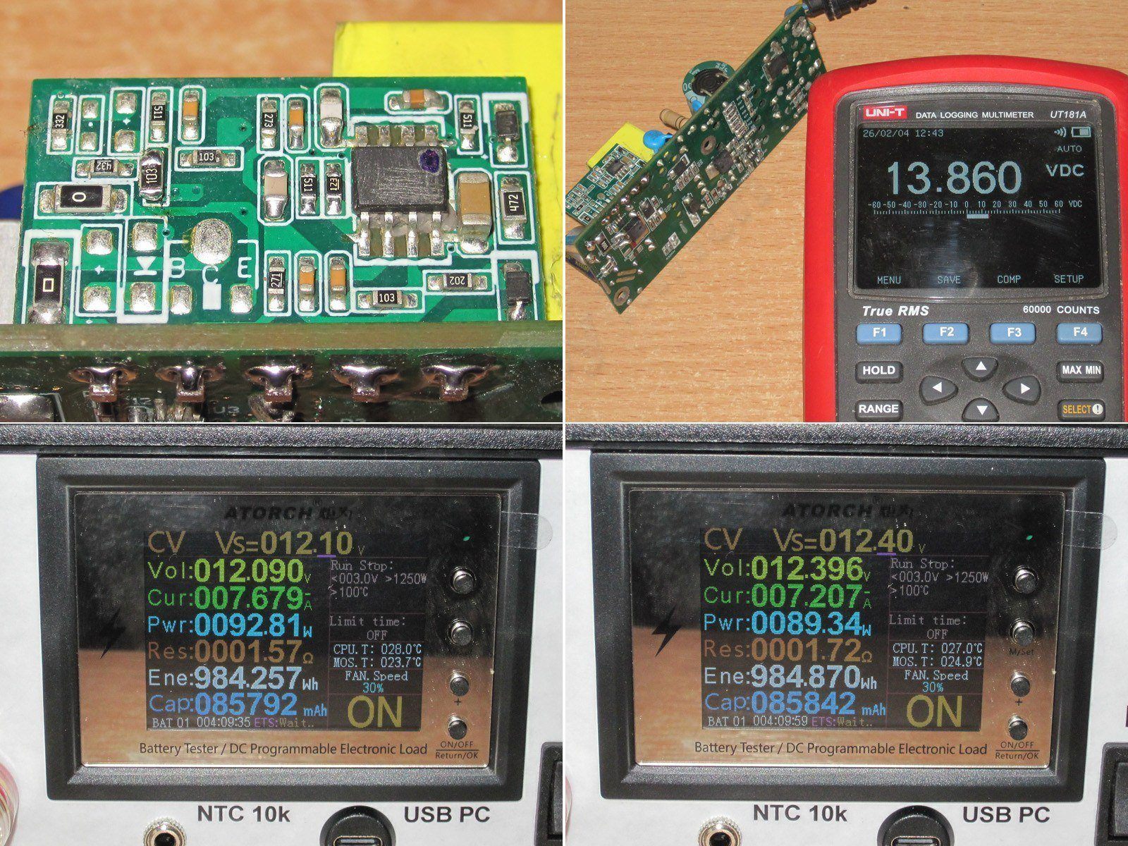
Just out of curiosity, I ran an experiment using a 100 W power supply. I soldered a 10 kΩ resistor in parallel with the lower resistor in the divider.
I got 13.86 V at the output. The calculated value should have been closer to 13.80 V, but never mind...
I loaded it in CV mode, and the current limiting works quite well. There is one drawback, though: the current depends on the output voltage, which is a little strange, and it’s lower than the output current I got in the earlier test, which was around 9.3 A.
I could take this further, but first, that’s beyond the scope of a power supply review, and second, I doubt anyone needs it. As for connecting the units in parallel, I think it should work. But keep in mind that if your load exceeds the power rating of a single unit, one power supply will most likely always operate in CC mode, while the other just supplements it. If you connect three units, two will operate in CC mode, and the third will just supplement them.

As for a varistor rated for 560 V peak or 400 V RMS, it won’t help in a situation like this.
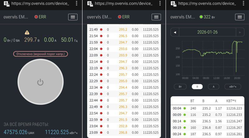
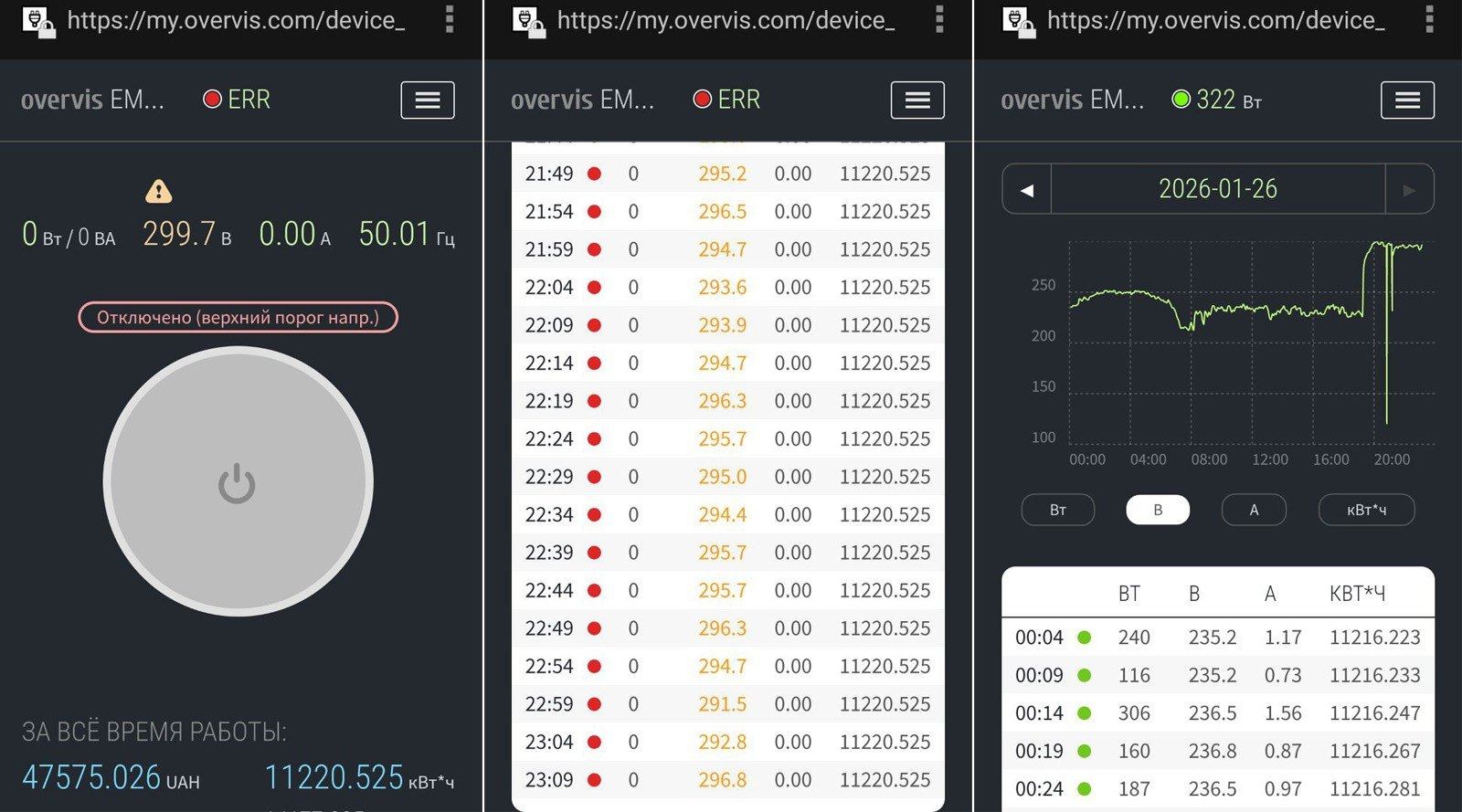
This is what it looked like across roughly half the city for six hours after yet another attack by idiots who “only target military infrastructure.” Yeah, right... Or like last night, when they shelled a combined heat and power plant and left 820 buildings without heat with temperatures outside at -25. Definitely not terrorists...
And this video is for those who don’t understand and only watch ROSTV - watch on YouTube
Just yesterday, if that piece of Russian shit had flown a little lower, it would most likely have hit our building (it ended up hitting another one; three floors burned out, thankfully with no casualties). This happens here pretty often: about a week ago, something similar flew past nearby, also at a very low altitude.
Conclusions.
I’ll sum up all the units at once. Overall, I liked them. There are a few things I’d improve or adjust, but the design approach feels pretty sound. I especially liked the separate current regulation; this is the first time I’ve seen that in units like these (although I once reviewed a 48 V power supply with this feature).
There are various shortcomings: the 60 W and 200 W units have too little input capacitance, while the 150 W unit’s power components get very hot. I liked the 100 W and 200 W units best. The 200 W version is particularly interesting, with its very good efficiency and sound circuit design.
That’s all for now. I hope this was useful, and thanks to Vitaliy for providing the samples.
As a reminder, if you want to stay up to date with new posts on the blog, I recommend following me on Instagram. I’ll post notifications about every new article there, and maybe write about other interesting things too - link to my account
You can also subscribe to updates and new articles on the Telegram channel - https://t.me/KirichBlog
This review will be fairly brief. I tried to bring all the tests in line with one “standard”; I think that will make things more convenient for you and easier for me.
I’ve actually had these for a very long time. At one point I even changed my mind about testing them and writing a review, but curiosity got the better of me—and it turned out to be worth it.
All the models come in metal enclosures, but these aren’t made from standard extruded profiles or U-shaped cases. They’re more like little trays with snap-on lids. Pretty neat and convenient :)
All the power supplies also come with connection cables. They’re not very long, but the wire gauge is perfectly adequate. They are pretty stiff, though, especially the output cable on the 200 W model.
These are 12 V power supplies rated at 60, 100, 150, and 200 W—in other words, the most common ratings.
As usual, let’s start with the smallest model: 60 W, or 5 A.
The board is secured inside with a couple of screws, but that’s fine considering the unit is normally potted. There’s also a plastic insulating sheet.
It looks reasonably tidy, though some areas seem oddly empty while others look a bit strange.
1. There’s an input EMI filter and a thermistor. It’s basic, but the essentials are there.
2. There’s even a varistor, rated for 560 V (about 395 V RMS), so it won’t provide overvoltage protection; it’s more likely there to suppress transient spikes.
3. Common-mode input choke.
4. There are two 15 µF capacitors on the input. In my opinion, that’s far too little.
While taking photos of the power supply, I realized what had seemed strange to me. Usually, in cases like this, the manufacturer sends units before they’re potted—that’s understandable and logical. But I was a bit stunned to find that this unit had been potted and then carefully cleaned out. I’m genuinely shocked.
So the person who sent these to me and I suspect that they’re actually made by another factory, and this one simply resells them.
Of course, that’s not a fact. But it seems less likely to me that someone took a finished unit, opened it up, and cleaned it out completely. What do you think? What are the possibilities?
1. The transformer looks perfectly adequate for the claimed 60 W, if not more.
2. And it uses litz wire—nice.
3. A small but welcome detail: the output has not only a polymer capacitor, but also a regular one right next to it, and it’s a decent Samxon part.
4. There’s a Y capacitor and... some kind of little board. Hmm...
Sure, I’ve seen power supplies with various submodules, but this clearly isn’t Bluetooth or Wi-Fi—it wouldn’t work inside a metal enclosure. There’s no mention of anything fancy like smart regulation, but the little board is there, and it clearly isn’t a TL431.
The chip marking has been rubbed off. I’d guess it’s an LM358, but I’m not certain. There are other possibilities, and judging by the unpopulated spots, the board may have been designed for models other than the 12 V version too, since there’s space for a basic voltage regulator.
I have no safety concerns, at least nothing obviously wrong stands out.
1. It’s curious that they’ve rubbed off the markings on every semiconductor, right down to the diodes. Paranoia? I think they did it specifically for the test samples.
2. On the output there are two diodes and... a shunt. Well, that’s clearly something new. I’ve seen this kind of thing before, of course, but it’s so rare I can hardly put it into words...
The first thing you notice is also the absence of the usual TL431, which gives me a few ideas.
First, the manufacturer has made some kind of universal module that handles the power supply’s entire feedback loop.
The module monitors not only voltage but also current. There’s also current monitoring on the primary side, which means the module is designed to operate in CC mode.
Why is that useful?
First, it provides overload protection—and better than monitoring the primary side, since that essentially limits power rather than output current.
Second, this design lets you connect power supplies in parallel, and they don’t even have to be the same power rating. You could use a 150 W unit and a 200 W unit to get, essentially, a 350 W power supply. Of course, this still needs to be tested, but everything points to that being possible. It depends on the current threshold and whether there’s a genuine CC mode.
All this raises the question: what chip could this be? I suspect it’s an AP4310, a dual op-amp combined with a voltage reference. I’ve come across it in this UPS
The actual capacitance of the input capacitors is close to the stated value, so no issues there. But the capacitance itself is questionable: even 30 µF is too little for a 60 W power supply, and that’s true even at 230 V, let alone 115 V, although the manufacturer specifies an operating range starting at 200 V. Still, it’s too little. Sure, it’ll work, but first, 100 Hz ripple will increase; second, the capacitors’ service life will be reduced; and third, if you install this power supply outdoors, as it’s clearly intended to be, freezing temperatures will cause real trouble.
No particular complaints about the output, especially since there’s also a polymer capacitor.
I used an EBC-A10H electronic load for testing. The board was simply lying on the table, and, as always, there’s a catch: it’s designed to be potted with compound, so it usually cools less effectively in this state. Though perhaps that actually makes for a more realistic test.
The test showed that the protection is set to a current of about 5.3 A, and this doesn’t depend on the power supply’s temperature. Someone will surely ask: where’s the CC mode?
Let me explain again: power supplies that operate in CC mode should be tested with an electronic load in CV mode, and vice versa. If you load a power supply with CC mode using an electronic load in CC mode, the current limiting should work exactly as it does here—that is, the voltage should drop to zero.
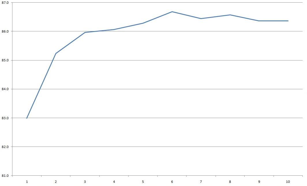
I measured efficiency from 0.5 to 5 A in 0.5 A increments, and in my opinion it’s pretty good for a power supply like this.
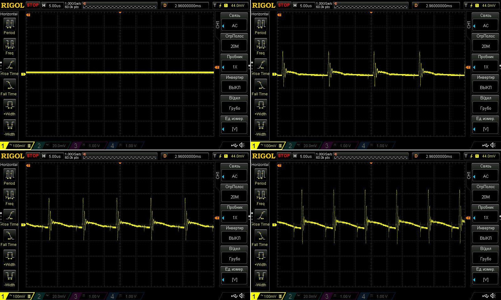
Ripple with no load and at 1.5, 3, and 5 A.
I wouldn’t call it low, but it’s not high either. I think the polymer capacitor helps a lot, so adding it was the right call.
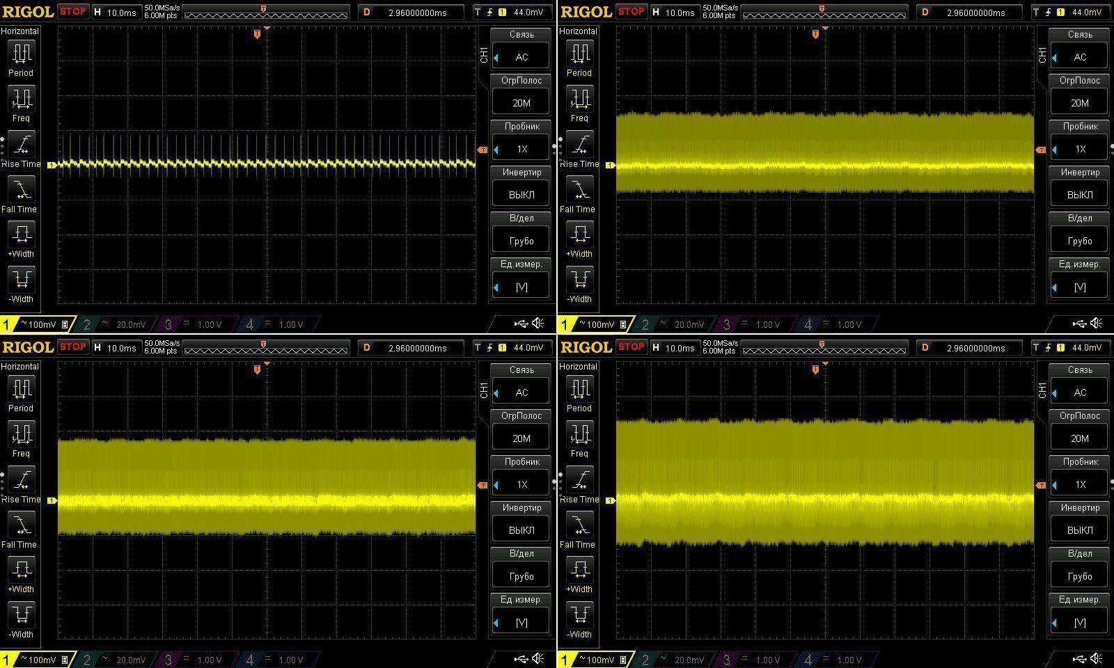
There’s almost no 100 Hz ripple despite the low input capacitance, but that’s probably thanks to the circuit design and the 230 V input.
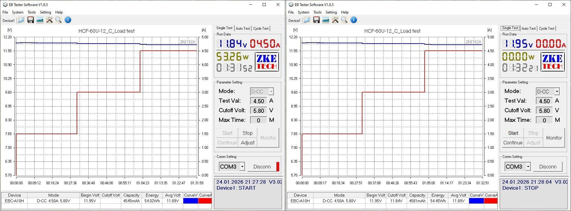
The load test was run in three modes: 1.5, 3, and 4.5 A. To be honest, I don’t remember why I capped it at 4.5 A instead of 5.
The output voltage does vary with load, but not by much. Some of that is due to the voltage drop in the output cable. There’s no temperature dependence.
Temperatures in all three modes. There’s no point commenting on the 1.5 A results, so I’ll go straight to 3 and 4.5 A.
At 3 A: transistor 77 °C, diodes around 85 °C, transformer 66 °C—excellent.
At 4.5 A: transistor 120 °C, too high; diodes 120 °C, also rather high; transformer 86 °C, perfectly fine.
Yes, the transistor and diode temperatures are on the high side, but I think it’s worth bearing in mind that air usually carries heat away less effectively than potting compound. So I’d expect temperatures to be lower once it’s in the enclosure and potted.
The second power supply: 12 V, 100 W, 8.33 A.
It’s structurally an exact copy of the previous one, just a little larger.
Everything inside is exactly the same, except there are now three screws :)
The board has also been cleaned of potting compound, but the board markings have been sanded off as well. That’s not paranoia anymore; it looks more like this isn’t the power supply manufacturer, but an intermediary.
1. The input filter is the same as on the previous unit.
2. The input capacitor is noticeably more substantial this time.
3. An optocoupler, and even a slot beneath it. Interestingly, there are two small capacitors on the high-voltage side here.
4. The transformer winding is also made with Litz wire.
5. On the output, there are two regular 1500 µF capacitors and one 1000 µF polymer capacitor.
6. And, just like before, there’s an additional board installed—in essence, a standardized submodule. A solution that isn't always applicable, but is quite convenient and makes it easy to scale power supplies with less effort.
As with the previous one, I have no safety concerns: there are clearances and slots, and even a ground connection.
The circuit design here is a bit more complicated, though.
An emitter follower has been added on the primary side to improve control of the high-voltage transistor.
On the secondary side, they used a synchronous rectifier. You can tell from the small chip in a SOT-23-6 package that controls the MOSFET.
The shunt here is 5 mΩ, compared with 10 mΩ in the previous one, but the output current is almost twice as high.
The input capacitor's actual capacitance is 106 µF, which is fine for 100 W of power. The output capacitance is 4300 µF, also fine.
The protection trips at around 9.3 A when cold and 9.1 A when hot, which seems a bit high if the idea is to allow parallel operation. In standalone mode, though, it's perfectly fine.
Efficiency is around 89%. Given the synchronous rectifier, that was pretty much expected. It was measured from 0.5 to 9 A in 0.5 A increments.
Ripple with no load and at 3, 6, and 9 A.
I wouldn't say 400 mV at maximum current is a lot, though of course less is always better. The main component is noticeably lower; the large peak-to-peak value is due to a short pulse. I think it would be noticeably higher without the polymer capacitor.
No issues at 100 Hz, but with an input capacitor like this, you'd expect it to perform well.
The test was carried out in four stages, at 2.5, 5, 7.5, and 8.5 A. The voltage regulation under load is good, considering the measurements were taken after the output cable, and the voltage barely depends on temperature.

Temperatures at 5, 7.5, and 8.5 A.
At 5 A: the transistor is at 70 °C, though the snubber diode nearby gets quite hot; the rectifier transistor is at 73 °C, and the transformer at 65 °C. All fine.
At 7.5 A: the transistor is at 94 °C, the rectifier transistor at 109 °C, which is a bit high, and the transformer at 84 °C, which is fine.
At 8.5 A: the high-voltage transistor is at 105 °C, which is a bit high; the rectifier transistor is at 128 °C, which is too high; and the transformer is at 91 °C, which is fine.
So basically, my main concern is the output rectifier transistor; it's running a bit too close to the limit. If you pot it with compound, things will probably improve, and it should even work at the maximum current of 9.1–9.3 A, but it's hard to say how it'll do in hot weather.
By the way, I've been wondering whether ChatGPT could be used for calculations like these.
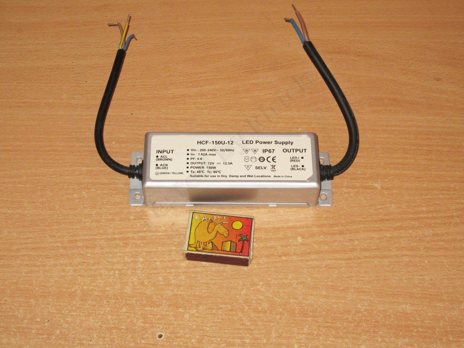
Third model: 12 V, 150 W, or 12.5 A
And once again, it's basically a larger version of the previous model.
150 W is a threshold power level: often too much for a flyback converter, but too little for other topologies, so I'm always curious to see what the manufacturer chose.
Here we have a single-switch flyback converter. In my opinion, 150 W is already pushing this topology close to its limits.
When I took the board out of the case, I also noticed a pair of thermal pads, several millimeters thick. They're installed in an unusual way, transferring heat through the plastic insulation.
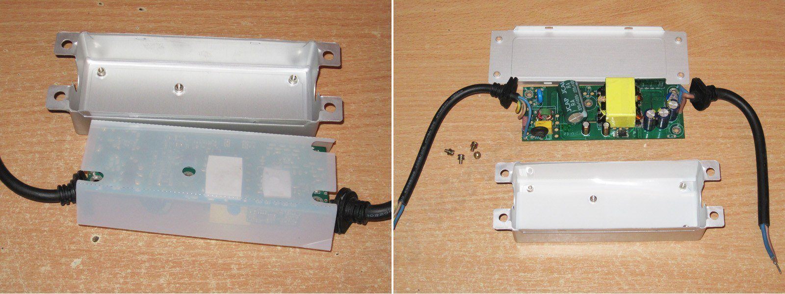
The board looks very much like the previous model. It even has the same two small capacitors, though there are more on the output side.
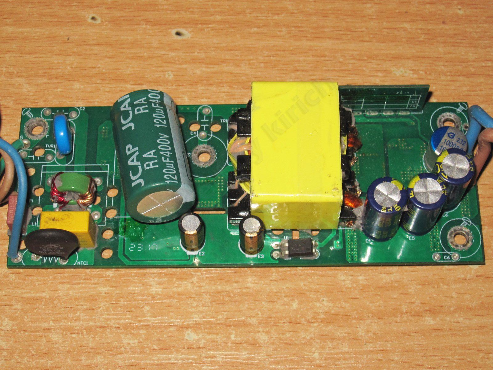
The filter, varistor, input capacitor, and the pair of small capacitors mentioned earlier—no, really, it's a copy of the previous power supply.
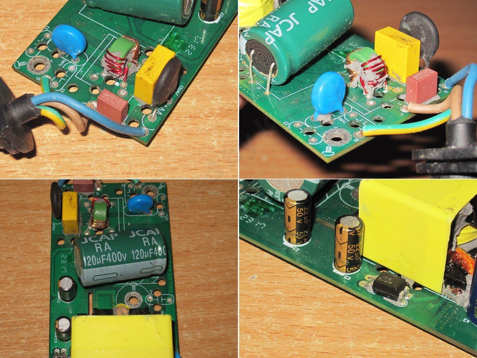
The submodule layout, Y capacitor, and litz-wire transformer winding—in essence, the manufacturer just scaled up the design a little and added one 1500 µF output capacitor. It was 2 × 1500 + 1000 µF; now it's 3 × 1500 + 1000 µF.
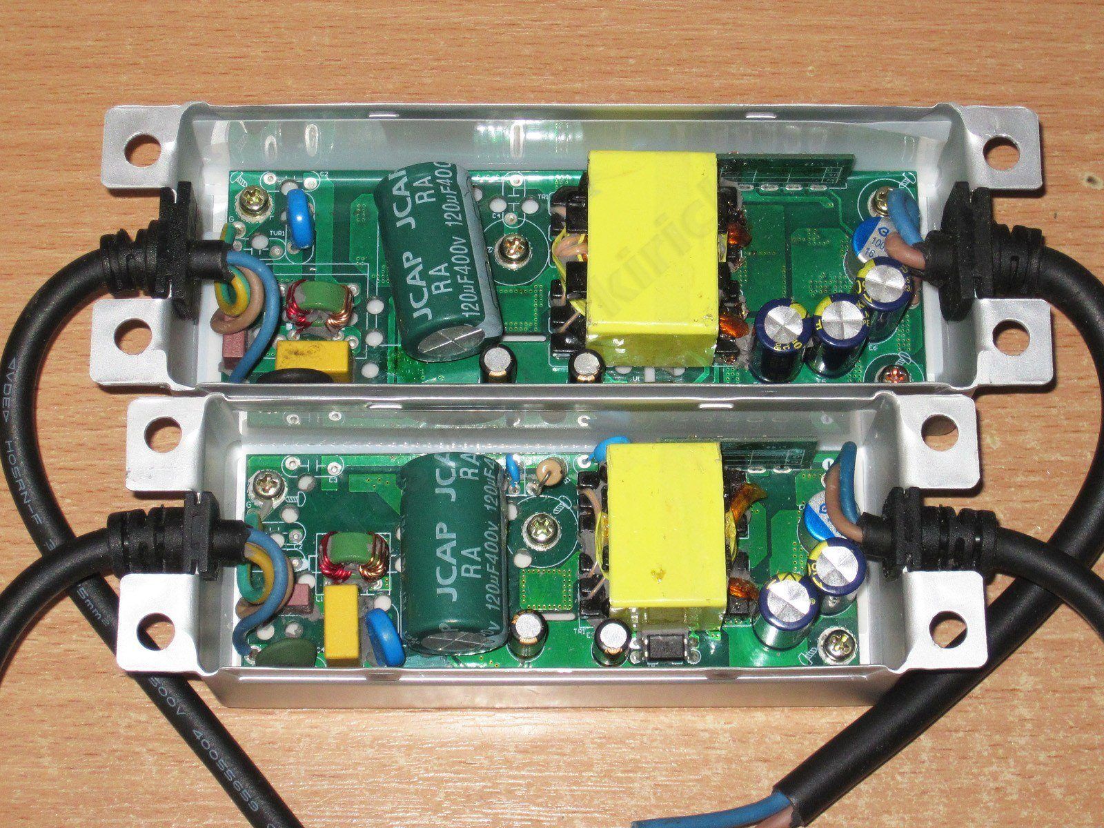
I even put them side by side in the end, because when you look at them separately, they really do seem like the same power supply.
But they're not. First, there are clearly some differences; second, the board itself is larger, though there's still a lot in common. In principle, this is a perfectly reasonable way to scale things up.
They decided not to replace the bridge rectifier, just added a second one in parallel—and also removed the markings from the bridge rectifier. Good grief, I'm shocked.... Apparently they gave the units to a student and told him, “Dig out the potting compound and erase the markings on everything you can see.” At least he didn't erase the markings on the resistors :))))
There are two thermal pads. The one on the right is obvious: that's clearly the output rectifier. But the one on the left isn't on a transistor, which would have been the usual arrangement.
I have no complaints about the board itself; overall, everything makes sense, and it was clearly laid out by someone with plenty of experience.
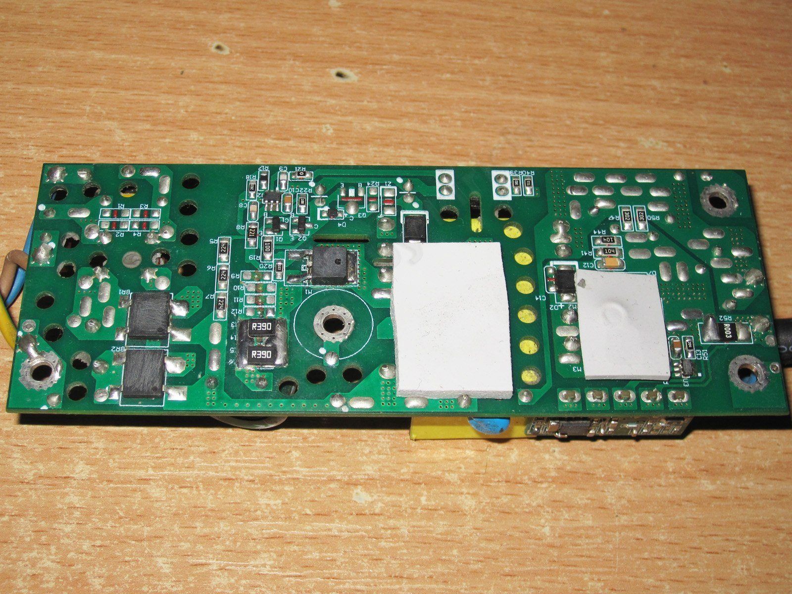
1. So, the pad was hiding a snubber. And yes, this is all correct: the more power you try to draw from a flyback converter, the harder the snubber has to work. So the designer made the right call in their own way by transferring its heat to the case. Doing it through plastic insulation, though... not ideal. Maybe they planned to add a window there.
2. The output uses a synchronous rectifier, but I somehow expected to see two transistors. There are even two footprints for them, so I suspect that was the original plan, but then an “optimizer” got involved. Actually, no—the space on the right is for a diode, not a transistor. Judging by the copper pours, you can fit either one transistor or two diodes, so maybe there was no “optimizer” involved after all.
The output current-sense resistor is 3 mΩ. If we assume the 60 W version had a 10 mΩ resistor, the expected current here is about three times higher.
The input capacitor is the same as in the 100 W version. That was fine there, but it's a bit undersized here.
The output has almost 6000 µF, which is fine in principle.
For obvious reasons, I used a different load this time. By the way, it's already been sent off to our military, so I'll have to build a new batch.
I used two connection setups. Efficiency was measured with a four-wire connection, as was the first test of the protection threshold. The long-duration tests also used four wires, but the load was connected to the output wires rather than directly to the board. The thing is, you have to move the board around during a long test, and I was worried something might short out and interrupt the test.
The protection trips at around 13.5 A and is practically unaffected by temperature. The top image shows the power supply cold, the bottom one hot; I even happened to catch the moment it shut down.
Efficiency was measured from 1 to 13 A in 1 A increments, and came out to about the same 89%. But you can see that efficiency drops at higher currents, which in my view is partly due to overloading the output rectifier. In other words, one transistor simply can't handle it, and its losses approach those of an ordinary Schottky diode.
The high-frequency ripple is about the same as on the 100 W version: around 400 mV peak-to-peak and about 120 mV for the main component. Unfortunately, power supplies with this kind of topology usually have noticeable ripple; it's inherent to the topology itself. But I should point out that for a flyback converter, and without an output filter, it still looks relatively good—which means the board layout is sound.
At 100 Hz, the results are about the same as on the 100 W version, with no issues.
The load test was run at 4, 8, and 12 A, for a total of about 1.5 hours.
The photos show the voltage with no load, at 4 A, 8 A, and 12 A at the start of each stage, then at 12 A at the end, and finally the voltage after removing the load.
You can see a slight change in voltage with load, about 40 mV. By the way, moving the feedback circuitry onto a submodule helps keep the output voltage stable as the temperature changes, since the feedback circuitry itself is farther from the heat source.
Temperatures at load currents of 8 and 12 A.
8 A — you can see the hot spot on the snubber. The transistor is at 82°C, which is fine; the rectifier transistor is at 93°C, also fine; and the transformer is at 73°C, which is perfectly acceptable too.
12 A — the snubber temperature is off the scale, above 130°C; that's a lot. The transistor is at 125°C, also too high. The rectifier transistor has likewise exceeded the thermal camera's 130°C limit, and the transformer is at 107°C. That's rather high.
It's clear that the scaling wasn't done very well: the snubber and rectifier transistor are obviously overheating, and the high-voltage transistor is getting quite hot too. The results should improve once the unit is potted and some of the snubber's heat is transferred to the case. Still, in my view, they could at least have added another output transistor. That would have made a noticeable difference by spreading the heat across two packages and reducing the voltage drop. The snubber would dissipate heat better if there were a cutout for a thermal pad, but the transformer is fine as it is; the potting helps it quite a bit.
And now the larger 12 V, 200 W model, rated at 16.86 A.
Visually, it's just a scaled-up version of the previous three.
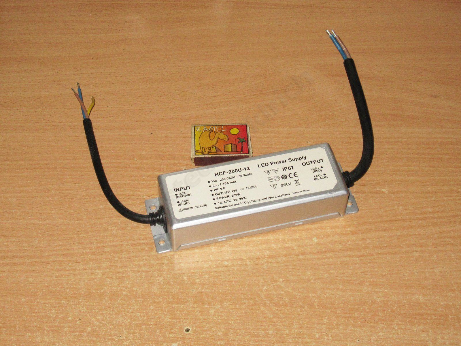
The layout is similar, but the differences are much more noticeable here—and, by the way, there are no thermal pads.
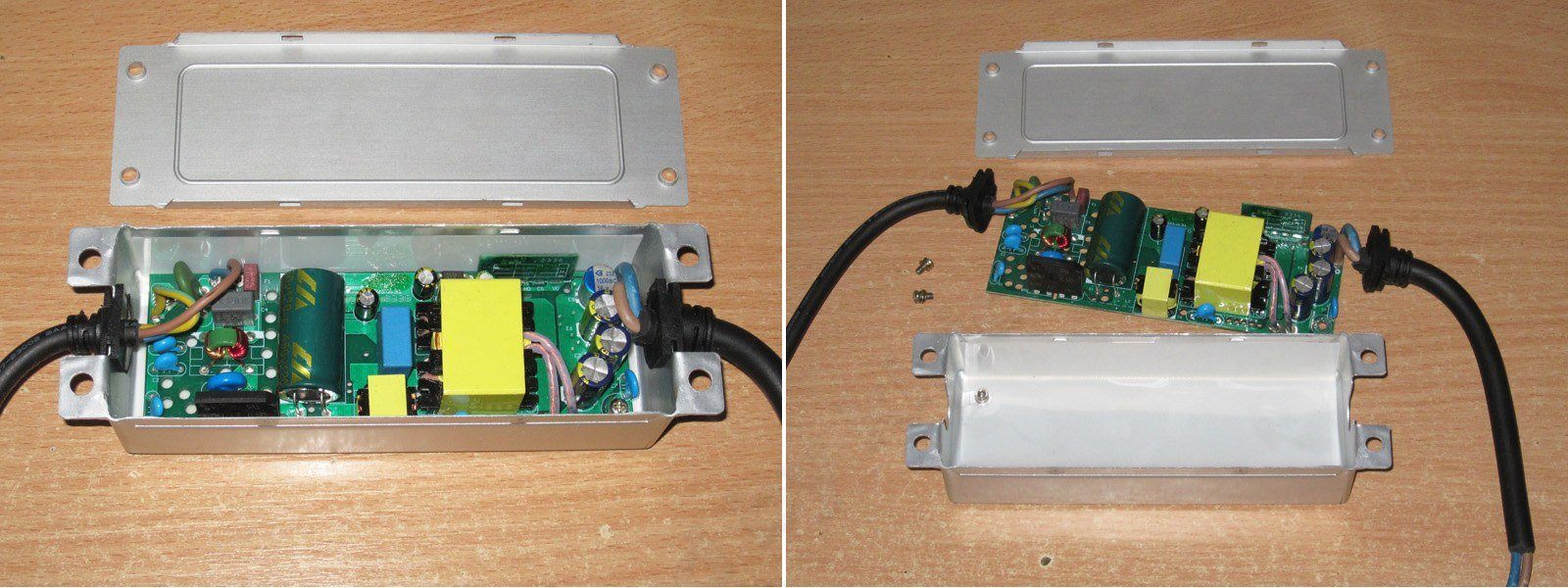
It's clear that this uses a classic LLC topology: an inductor, a transformer, and a capacitor.
As with the previous models, the board layout is fairly spacious, which is good.
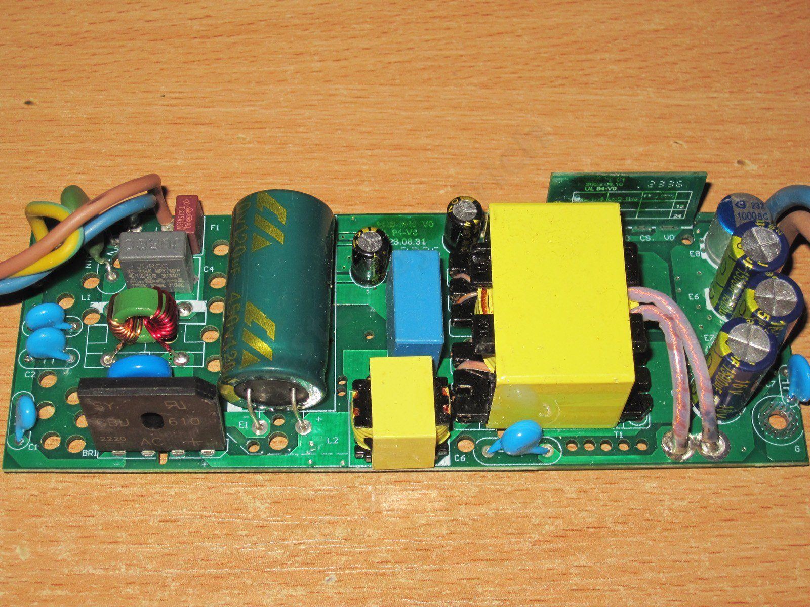
1. The input filter is a little better than on the previous models: several Y capacitors have been added, and a more powerful bridge rectifier is used. The input capacitor, though, is the same as in the 100 W and 150 W versions, which is a bit small... But given that the specified input range starts at 200 V, it should be adequate, just barely.
2. The classic LLC topology itself.
3. Interestingly, in addition to the two capacitors on the primary side, there's another small one on the secondary side.
4. Interwinding Y capacitor.
5. On the output, there are three standard 1500 µF capacitors and one 1000 µF polymer capacitor, which is perfectly adequate for this topology.
6. There's an additional capacitor between the output and the case.
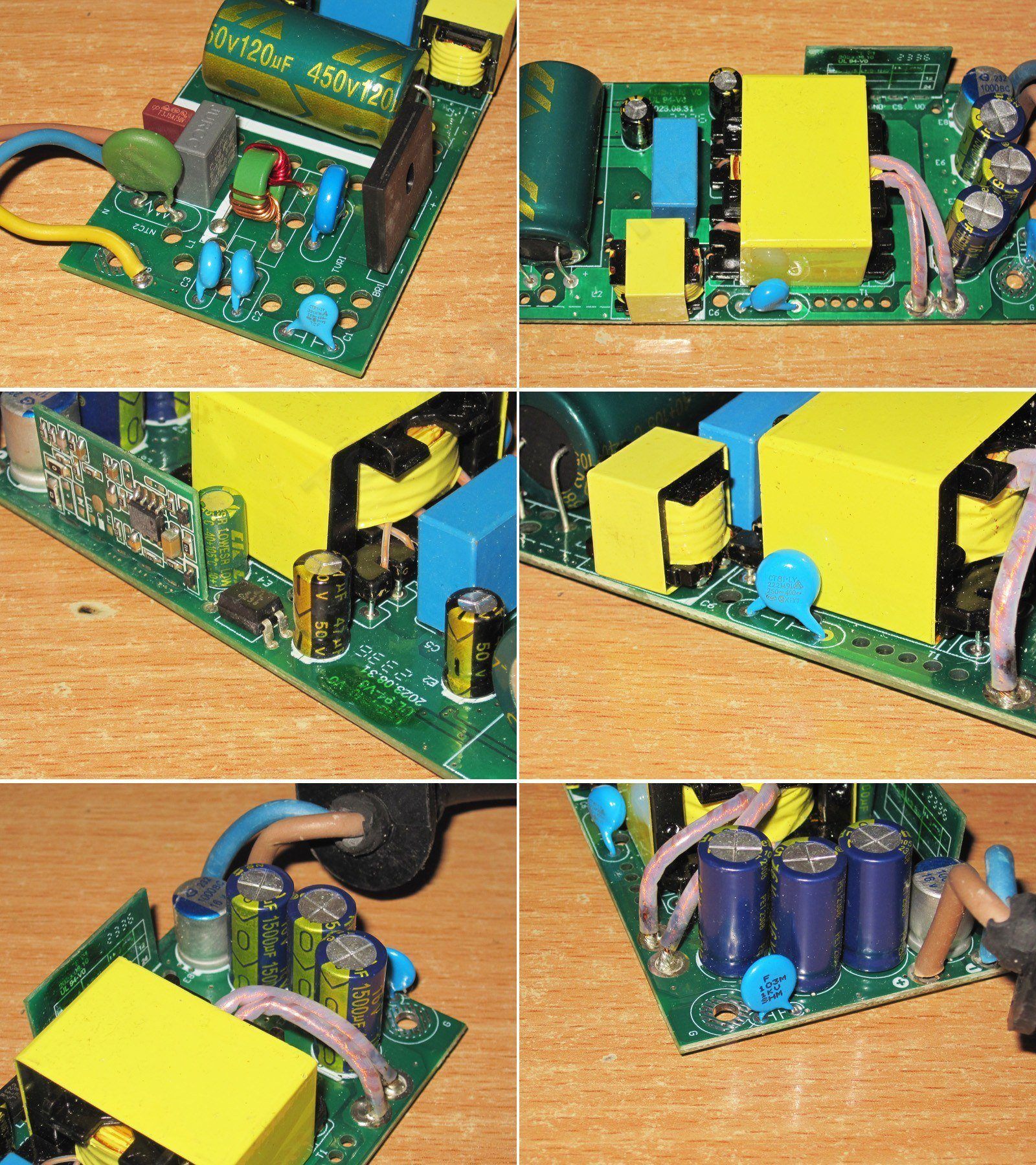
No safety-related issues with the PCB layout. You almost want to say, “See, they can do it when they want to...”
Oh, and I almost forgot: this is the only one of the four power supplies that wasn't cleaned of potting compound—it arrived clean.
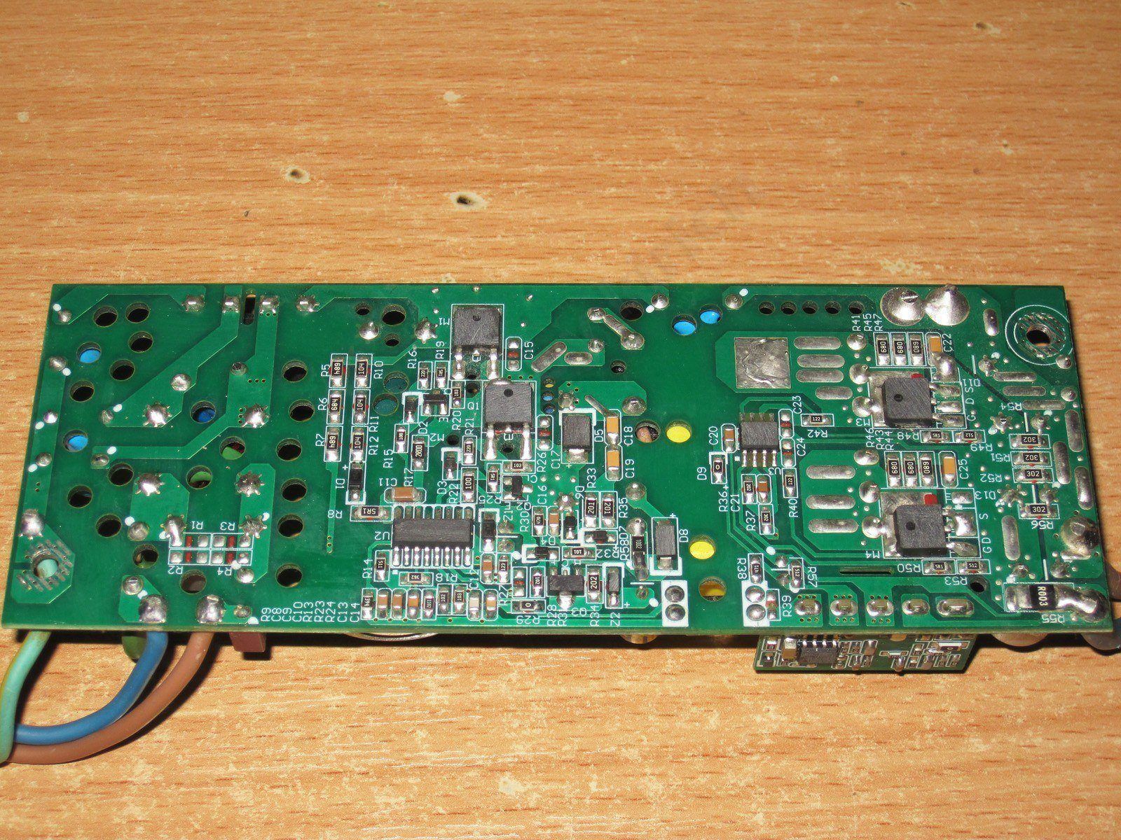
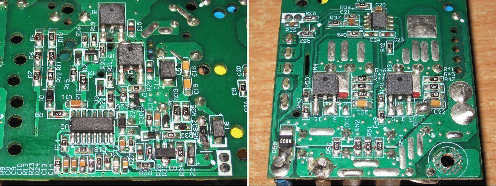
1. All the component markings have also been removed from the input section, but I think the controller is something like a TEA2016, since there aren't that many LLC controllers. Interestingly, I couldn't find a current-sense resistor on the primary side.
2. On the output side, there's a 3 mΩ shunt and two synchronous rectifier transistors. I wonder if they could get it down to just one? :)
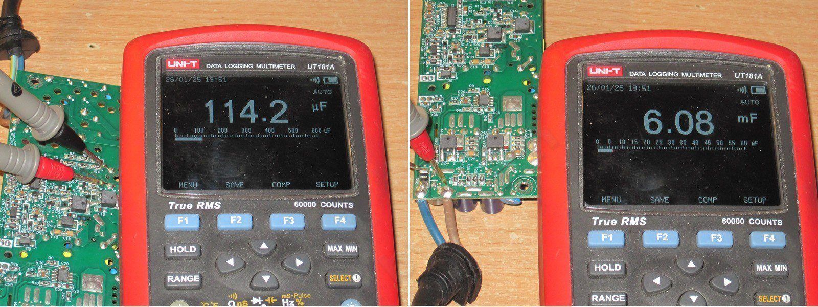
Interestingly, the input capacitors in the 100 W and 150 W models had an actual capacitance of 106 µF, while this one, which looks identical, measures 114 µF.
About 6000 µF on the output, no complaints there.
The protection trips at around 18–18.1 A, regardless of temperature.
I measured efficiency from 1 to 18 A in 1 A increments. Across almost the entire range, I got around 90–91%, and the efficiency curve is practically flat.
Ripple at no load and at currents of 6, 12, and 18 A.
The high-frequency ripple looks great: even the full swing is only 150 mV, and most of it is within 50 mV. But as I often point out, that's mostly down to the topology; the same goes for power supplies using a half-bridge topology.
The odd no-load waveform was an accidental result, most likely caused by the “green” mode.
At low frequencies, though, we can see clear 100 Hz ripple. It's not critical for most loads, but this power supply isn't suitable for powering audio equipment.
The load test was run at 5, 10, and 15 A. Since the power supply performed quite well, I then raised the current to 17 A, drawing over 200 W (accounting for the voltage drop and cable losses, that's 200 W at the load).
The output current probably has very little dependence on the load, since what we're seeing here also includes the voltage drop in the output cable. There's practically no temperature dependence: it was 11.95 V and became 11.94 V.
And, of course, the results of the load test. The test lasted about two hours in total, so the power supply had plenty of time to warm up.
Results at 10, 15, and 17 A:
10 A — transistors at 63 °C, rectifier at 60 °C. The rectifier controller actually ran hotter, at 62 °C. The transformer was at 60 °C. No complaints at all.
15 A — transistors at around 92 °C, which is fine; rectifier at 86 °C, good; transformer at 76 °C, excellent.
17 A — transistors at 100 and 110 °C, right on the limit, with the outer one running hotter. The rectifier transistors were at 94 and 105 °C, with the right one hotter; the transformer was at 90 °C, which is good.
As for the temperatures, I can say that, given the lack of heatsinks, the results are actually quite good. This is the power supply I was referring to in my review of the 240 W model in a recent post. That is, There’s a 240 W unit with large heatsinks, and I wouldn’t say it runs much cooler than this 200 W model, which uses polygon-shaped heatsinks on the circuit board.
I think it would work even better if you filled it with potting compound to spread the heat and transfer it to the case. All in all, I think the results are pretty good.
Later, I decided to find out what chip was on the submodule. As it turned out, it really is the familiar AP4310, which means there’s a full-fledged CC/CV mode here.
Just out of curiosity, I ran an experiment using a 100 W power supply. I soldered a 10 kΩ resistor in parallel with the lower resistor in the divider.
I got 13.86 V at the output. The calculated value should have been closer to 13.80 V, but never mind...
I loaded it in CV mode, and the current limiting works quite well. There is one drawback, though: the current depends on the output voltage, which is a little strange, and it’s lower than the output current I got in the earlier test, which was around 9.3 A.
I could take this further, but first, that’s beyond the scope of a power supply review, and second, I doubt anyone needs it. As for connecting the units in parallel, I think it should work. But keep in mind that if your load exceeds the power rating of a single unit, one power supply will most likely always operate in CC mode, while the other just supplements it. If you connect three units, two will operate in CC mode, and the third will just supplement them.
As for a varistor rated for 560 V peak or 400 V RMS, it won’t help in a situation like this.
This is what it looked like across roughly half the city for six hours after yet another attack by idiots who “only target military infrastructure.” Yeah, right... Or like last night, when they shelled a combined heat and power plant and left 820 buildings without heat with temperatures outside at -25. Definitely not terrorists...
And this video is for those who don’t understand and only watch ROSTV - watch on YouTube
Just yesterday, if that piece of Russian shit had flown a little lower, it would most likely have hit our building (it ended up hitting another one; three floors burned out, thankfully with no casualties). This happens here pretty often: about a week ago, something similar flew past nearby, also at a very low altitude.
Conclusions.
I’ll sum up all the units at once. Overall, I liked them. There are a few things I’d improve or adjust, but the design approach feels pretty sound. I especially liked the separate current regulation; this is the first time I’ve seen that in units like these (although I once reviewed a 48 V power supply with this feature).
There are various shortcomings: the 60 W and 200 W units have too little input capacitance, while the 150 W unit’s power components get very hot. I liked the 100 W and 200 W units best. The 200 W version is particularly interesting, with its very good efficiency and sound circuit design.
That’s all for now. I hope this was useful, and thanks to Vitaliy for providing the samples.
This page was found when searching for:
5
5
This model is included in the summary table: Comparison of power supplies: ripple, efficiency, and temperature rise
The figures from this review are in the measurement database: Power supplies
Calculate manuallyAll calculators
Discounted products
You may be interested in



Discounted products
Support the project
All the content on the site and the advice are free, but we’d be grateful for your support of the project and the channel!
Comments1
Discuss on the forumHave a question or some experience to share? Discuss the article with the author and readers: the forum is a convenient place to share schematics and photos.
Go to the forumOnly registered readers can comment. It takes a minute to sign up, and you can log in with the same account you use on the forum.
Log inRegister
Comments are published in their original language.