
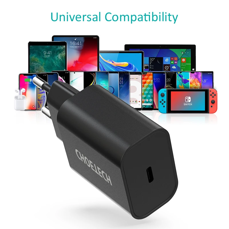
Choetech Q6006 power supply (charger) with 61 W PD support and GaN technology
$20 с кодом
Inspection, tests, comparison, measurements—as usual.
For the sale, the seller provided the promo code MMLFWBSIS2I2, which gives you 5 off 24, so you can get this charger for 20 dollars.
A while ago, I published a review of a pretty decent 60 W power supply. It was reasonably well built, worked reliably, and supported various protocols. But not long after that, I was sent another, more "modern" model, built using GaN components. I had actually arranged to review the 100 W version, since that's the one readers had been asking me about, but I ended up receiving the less powerful Q6006 instead.
On the other hand, the Q6006 is almost identical to the Q4004: their rated power differs by just 1 W, 61 versus 60. So it might be interesting to compare the two—a classic model and an updated one.
The package contained a box with the charger (power supply) and a cable. All the necessary technical specifications are printed on the packaging, which also seems sturdy enough to me. The charger itself is sealed in a bag that can only be opened by tearing it, so you can tell nobody has used it before you.

I wanted to start the review by testing the included cable, but when I took a closer look, I realized I'd already had exactly the same cable. A compatibility test with PD at 100 W confirmed it. You can read more here.

As before, the package includes the power supply itself, a manual, and a piece of paper that I've already shown how to use.

Nothing interesting in the manual: technical specifications and a brief description in English.

The first thing I noticed was the size: it's noticeably smaller than the previous model and, to my eye, looks neater.

You can get an idea of its size by comparing it with a matchbox.

The case also lists all the necessary specifications.
The previous model had a detachable plug, so you could use either the European-style plug or the flat pins. This one has a fixed plug. I think that could be a drawback for people who travel often, but for me it's more of a plus, since the design is more solid this way.
They've also added a power indicator next to the output port. It glows very dimly, and its brightness depends on the output voltage. Since I don't like bright indicators, this one is just right.

And now for a visual comparison with the previous model.
1. It's clearly smaller.
2. The only difference in the specifications is the last item: the new model adds a 20.3 V mode, which accounts for the "extra" 1 W of power.
3. There's almost no difference in thickness.
4. The pins on the new model's mains plug are correctly angled slightly inward, unlike the previous model, where they were parallel.

The product page also compares it with the regular version.

I couldn't find a clear list of supported protocols; the product page only has this image.

Well, let's connect a tester and see what it can do.
As it turns out, not much. Technically, it only supports Quick Charge and Power Delivery, and QC only goes up to 12 V.
I tried controlling the protocols directly, since auto-detection doesn't always work correctly. But no: QC really does max out at 12 V, with a minimum of 4.46 V. If you try to lower it further, the charger "reboots".
It also doesn't support Huawei FCP, SCP, or Samsung AFC.
It does support PD, though. The tester identified it as version 2.0, so it doesn't let me adjust the voltage in small increments. But it does show that the power supply can indeed output 20.3 V, although I don't remember Power Delivery specifying such an unusual voltage.

Out of curiosity, I checked it with two more testers: my main 1276 and the new Fnirsi FNC88.
The first one showed basically the same thing, but identified PD as 3.0. The FNC88, however, decided QC only went up to 9 V and that Huawei was supported, but it wouldn't set 9 V in the second mode. It also identified PD as 3.0, but still didn’t allow fine voltage adjustment.

For the tests, I had to butcher one of the USB testers again so I could solder onto the power rail before the shunt. No-load power consumption is 0.4 W—pretty efficient, though I’ve come across power supplies with even lower consumption.

Load tests.
First, the “default” voltage—that is, what the output provides when the power supply isn’t given any commands. For power supplies like this, the standard is 5 V.
It’s a little high: 5.07 V with no load. There’s compensation, and as the current increases, the voltage rises to 5.34 V at 3 A and 5.4 V at 3.6 A, after which the protection kicks in.

Next, QC. At 5 V, everything was as shown above, but at 9 V the power supply behaved mysteriously: after the current reached 3.4 A, it dropped the voltage to about 6 V, and only shut down completely at 4.5 A.

At QC 12 V, the results were almost identical, except it shut down at 4.7 A. Very unusual behavior: the protection seems to kick in, but it looks rather strange.

Interestingly, everything works normally in PD mode. There’s also voltage compensation as the load current increases.

And the last mode: 20.3 V.
There’s no compensation here. The voltage started at 20.37 V, then dropped to 20.22 V at the rated current of 3 A. The protection kicked in at 3.6 A, as it did in all the other modes where the voltage doesn’t “float” under overload.

I decided to start the thermal test at 3 A and 5 V, but soon realized there was no point in testing it that way.

According to the measurements, the charger was dissipating about 3–3.5 W, so it barely warmed up. Even at the hottest spot, the temperature was only 40 degrees.

So I simply set the output to the maximum voltage of 20.3 V, set the maximum rated current of 3 A, and left it running for about an hour.
During the test, the voltage dropped slightly from its initial 20.208 V to 20.11 V.

In the end, I got 64 degrees on top and 73 on the bottom, with the power supply positioned almost horizontally. I’d say the temperature is fine.

Ripple was measured at the USB tester’s contacts.
1. With no load, the power supply runs at a reduced frequency and makes a slight noise, but you can only hear it if you put your ear almost right up against the case.
2, 3, 4. Next, tests at 3.3 A and 5, 12, and 20.3 V. The ripple amplitude barely changes, staying around 120–140 mV, but the frequency does change: it’s higher at a higher output voltage (and therefore higher power).
The ripple amplitude is a little high at 5 V, but within the normal range at the other voltages.

After the tests, I took the power supply apart, of course.
It’s relatively easy to open: a knife, a small hammer, and a little time. Only the side edges were mostly glued; the area around the mains plug and the inserts with the indicator and USB socket were not glued.

There will be some difficulty separating the two halves, though, since they are also glued to the internals with sealant.

The internals are covered on the sides by copper shields, which also serve as heatsinks and are soldered to the circuit board.

Though it would be more accurate to say that only one plate serves as a heatsink—or even as a heat spreader: the one on the circuit-board side. It has a large piece of thermally conductive rubber covering almost the entire board.


What's more, this thermally conductive rubber was attached with sealant, so no matter how carefully I tried to remove it, I still damaged it in places.

The layout inside the power supply is very cramped. For some reason, it even reminded me of laptop power supplies, where it feels like the components are practically packed into compact cases before everything is filled with sealant.

The input has a fuse and a proper input filter, but there is no varistor or thermistor. The former isn't that critical, but without a thermistor you can hear noticeable "clicks" when switching it on. In any case, having this kind of filter already says a lot—for example, that they didn't cut corners here. The lack of a thermistor can be explained by the pursuit of high efficiency.

1. There is a 410 pF interwinding capacitor, as well as an X capacitor
2. The input filter uses four Aishi capacitors rated at 22+22+22+27 µF, for a total capacitance of 68 µF. Yes, I've written before that their capacitors are relatively good quality, but their high-voltage ones almost always have lower-than-rated capacitance. It's also odd to see a combination where one capacitor has a slightly higher capacitance than the others.
3. The output has an 820 µF, 25 V polymer capacitor, with a tiny LED tucked in beside it.
4. There is another capacitor in parallel with the output capacitor, also polymer, but rated at 100 µF. They are connected in parallel; personally, I think they could at least have added a small SMD inductor.

The Type-C connector board has small ceramic capacitors and an RU3089M switching transistor RU3089M with an on-resistance of 2.4 mΩ, which switches power to the load. I've written before about why this transistor is needed: ideally, when the output is overloaded, the current should be cut off by disconnecting the output, not by shutting down the PWM controller.

On the other side is the WT6636F QCPD controller; the previous version used a WT6615F.

At the same time, the power supply version from On Semiconductor also lacks QC at 20 V :(, but it does support PD at 20 V, 4.5 A

There are more components on the underside. I didn't redraw the circuit; I don't think it would be particularly useful here.

1. The input bridge rectifier, with a pair of resistors beside it to discharge the X capacitor. I once came across a complaint that the plug gives you a "tingle" when you unplug the power supply from the outlet. This usually happens when these resistors are missing. They are present here, and there are at least two in series, as there should be (three would be better), but their combined value is rather high at 3 MΩ.
2. The synchronous rectifier transistor AON6220, rated at 100 V, 48 A, 6.2 mΩ—very good for a current of 3 A.

And now for the much-talked-about GaN. Of course, this is actually a controller with an integrated transistor made from gallium nitride—or, more precisely, in this case, a high-voltage GaN transistor on a sapphire substrate.

The SC1933C controller from Power Integrations is highly integrated and includes:
1. A PWM controller with protection circuitry.
2. A high-voltage transistor
3. Galvanic isolation
4. Feedback circuitry
5. Synchronous rectifier control circuit.
Interestingly, although the manufacturer lists all the key features, including compensation for voltage drop in the cable, nowhere do they draw attention to the fact that the high-voltage transistor uses GaN technology.

Even in the high-voltage section block diagram, it is simply labeled Sense FET.

I was beginning to think it was another scam, but the press releases did mention the new technology, describing this very chip and even showing photos of its internals.

There were even more detailed photos there, for the connoisseurs :)
High-voltage transistor structure

The “cold” side circuitry, with the feedback and so on.

I really like Power Integrations products. The company became widely known not only for its well-known TOP series controllers (standard power supplies), LinkSwitch (compact, low-power power supplies), and DPA (PoE solutions), which I've been using for a long time and very often—even in simple power supplies, for example. I once posted a description of how to build those: one, two.

The only thing that threw me off was that I didn't know the company had changed its logo. I hadn't bought their chips for a while, and the logo used to look different. I wonder if anyone can tell which one is genuine and which is counterfeit :)

But in my opinion, the company became even better known for publishing not just datasheets, but also application notes based on real devices. They show not only the schematic, but also the circuit board, a parts list, lots of test results, and even instructions for making the wound components! I learned a lot myself from these application notes and their software for designing power supplies.
The photo shows a screenshot from an application note for a similar chip (there are more), but, incidentally, I never did find a complete datasheet for the chip used in the power supply under review.

Unfortunately, it's not possible to measure the component temperatures accurately: in its original state, I couldn't get inside, and taking it apart partially compromised the cooling system. Still, I gave it a try. I covered the power supply with a small lid to reduce cooling and loaded it at 3.3 A and 20.3 V, giving an output power of about 67 W, or 110% of the rated maximum.
1. After 5 minutes, I measured the board temperature. The controller chip was the hottest, at about 65 degrees.
2. I ran it like that for another 15 minutes or so, and the controller reached 79 degrees.
3. The transformer temperature was 71 degrees.
The test isn't entirely rigorous, of course, but I think the temperatures are fine.

And here's a question that comes up often: what about the efficiency of these power supplies? Some buyers expect it to be incredibly high.
In reality, efficiency is high, but predictably not much higher than that of conventional power supplies. It reaches 90–91% at power levels close to maximum, with output voltages of 12–20 V.
The horizontal values correspond to load currents from 0.3 to 3.3 A in 0.3 A increments.

A conventional power supply is slightly less efficient, around 88–91%, but it only reached 91% at 100–110% load and maximum voltage.
As they say, we live off those two percentage points :)

So what does GaN offer?
For designers: better component characteristics and the ability to operate at higher frequencies and temperatures.
For users: slightly higher efficiency, which makes it possible to build more compact power supplies.
For marketers: well, they really went all out here, drawing pretty pictures and promising efficiency of almost 100% :)

In reality, you could say these power supplies are a little more interesting than conventional ones, but in my opinion, not enough to warrant such a big PR campaign. So if you're willing to pay extra for compactness, you can buy one of these chargers. If you'd rather save money, you can get a conventional one; I don't think the difference will be very noticeable.
It's inconvenient to use the power supply disassembled, for obvious reasons, so I'm putting it back together.
1. The thermal pad won't work as well now, of course, since it doesn't sit as snugly as before, but I don't think the difference will be significant.
2. I solder the copper shields back on.
3. Then everything needs to be wrapped tightly with tape. I used the same kind as the original. I use this tape in various widths for insulation when making transformers.
4. I checked that the whole assembly fits in the case and that the cover closes. In fact, I should have removed the leftover sealant; it meant I had to squeeze the case hard during assembly. I didn't do that, and I should have.
5. I ran glue along the seam, then clamped the whole assembly, placing the supplied paper strips underneath.
6. To speed things up, I decided to warm the unit a little by charging my phone with it. Of course, it would have been better to check the output with a USB tester after gluing it together, just in case "something went wrong".

That's about it. I used a little too much glue, and a thin bead squeezed out in a few places. But it's perfectly fine for home use, and I don't need anything more.

So, what can I say about the power supply under review?
The good points: quality components, a well-thought-out design, stable operation, no overheating, PD support at 20.3 V and 3 A, with 3.3 A actually sustainable over the long term, and a compact size.
What I didn't like: somewhat odd behavior of the protection in QC mode, QC support only up to 12 V, and a limited choice of supported protocols.
I really don't understand how they could implement PD at 20 V but not QC at 20 V. I can't make sense of it. After all, this depends essentially only on the controller implementation, since the power supply can handle it in hardware.
In short, I liked the power supply technically, but as I wrote above, you could easily replace it with the previous Q4004 version, which costs less, supports more protocols, has the same power, slightly lower efficiency, and a larger size.
The power supply currently costs $26.99, with a sale price of $25.06 expected. The seller also asked me to add a link to the ichoetech website, where you can buy this power supply for $28.00 with the SAVE20WH coupon, though I don't see the point of doing that...
That's all from me. I hope you found this useful.
$20 с кодом
This page was found when searching for:
что такое блок питания с pd, pd8002 gan обзор, choetech 100 вт gan, sc1139dg зарядное устройство
что такое блок питания с pd, pd8002 gan обзор, choetech 100 вт gan, sc1139dg зарядное устройство
The figures from this review are in the measurement database: Chargers
Calculate manuallyAll calculators
Discounted products
You may be interested in



Discounted products
Support the project
All the content on the site and the advice are free, but we’d be grateful for your support of the project and the channel!
Discuss on the forumHave a question or some experience to share? Discuss the article with the author and readers: the forum is a convenient place to share schematics and photos.
Go to the forumOnly registered readers can comment. It takes a minute to sign up, and you can log in with the same account you use on the forum.
Log inRegister