
Sealed HCF Series Power Supplies, Revised Version
I've already reviewed some models in this series. Back then, we were given “drafts”—just the circuit boards. This time, the units differ from the production models only in that they aren't potted, and they also include the changes we recommended.
As a reminder, to keep up with new posts on the blog, I recommend following me on Instagram. I'll post notifications about all new posts there, and might also write about something interesting from time to time: link to account
You can also subscribe to updates and new articles on the Telegram channel - https://t.me/KirichBlog Note that discussions of reviews and articles are enabled on the channel, as is general chat. I recommend it.
As I've written before, we're trying to get power supplies that offer the best balance of quality and price. So we take some basic models, test them, send our recommendations to the factory, and they incorporate the changes into the production units.
Today's article is a case in point.
The goal is simple: with a minimal increase in the product's price, we want to get:
1. Better safety, through certain components and circuit board layout.
2. Better reliability, meaning a longer service life and operation over a wider temperature range.
3. Better power quality. For example, what's the point of a power supply with high efficiency and excellent reliability if it dumps ripple into the load?
That's exactly why we make these optimizations. But people sometimes mean different things by “optimization.”
One kind of optimization is to cut the price by removing the input and output filters and using components that are pushed to their limits. Sure, the price goes down, but quality takes a serious hit.
Another kind of optimization, for example, is replacing a component mounted on a heatsink with a more efficient one. Interestingly, this often has almost no effect on the price: even if the new component costs more, you may no longer need a heatsink, and the component being replaced wasn't free either. The usual bonus is higher efficiency, which means less heat and better reliability.
We stick to the second kind of optimization, but unfortunately, we often see the first kind in our market—and elsewhere.
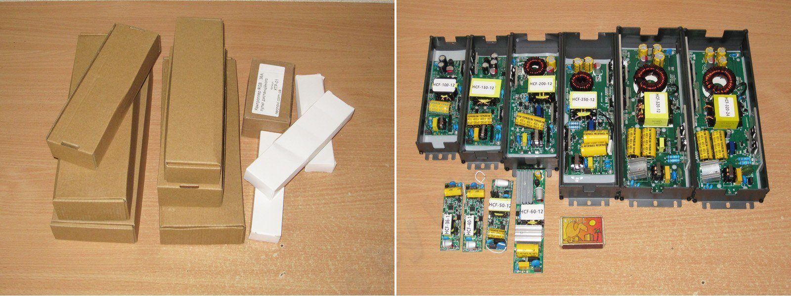
So, today's article will cover 8 power supplies rated at 36, 60, 100, 150, 200, 250, and two at 320 W.
As you can see in the photo, there are clearly more power supplies than that. After testing, we simply didn't like the 50 W model, so it was replaced with a 60 W version. As for the 40 W model, you'll see why as you read on.
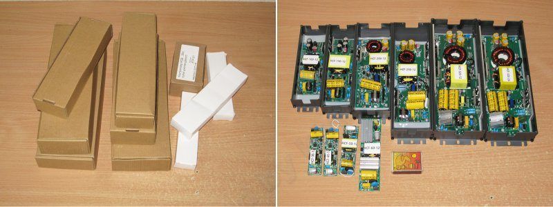
Someone will of course say, “What's the point if the Chinese can just do whatever they want, especially since the unit is sealed?”
No. From time to time, we can randomly select a unit from a batch, take it apart, and compare it with the sample—especially since we have detailed photos. If they substitute anything, we file a complaint with the factory. We need consistency.
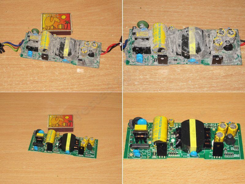
And of course, I'll start with the 36 W model, i.e. 12 V, 3 A. - link
I'll show this model alongside the 40 W version, but I didn't even test the 40 W one because I didn't think it was worth doing.
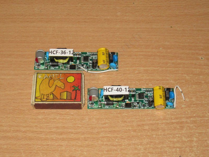
I think this photo makes it clear why I tested only the 36 W model: the boards are identical. What's interesting is that the Chinese set different prices for them, which is reflected in the store price.
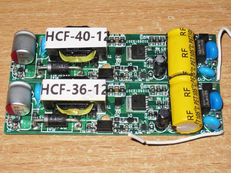
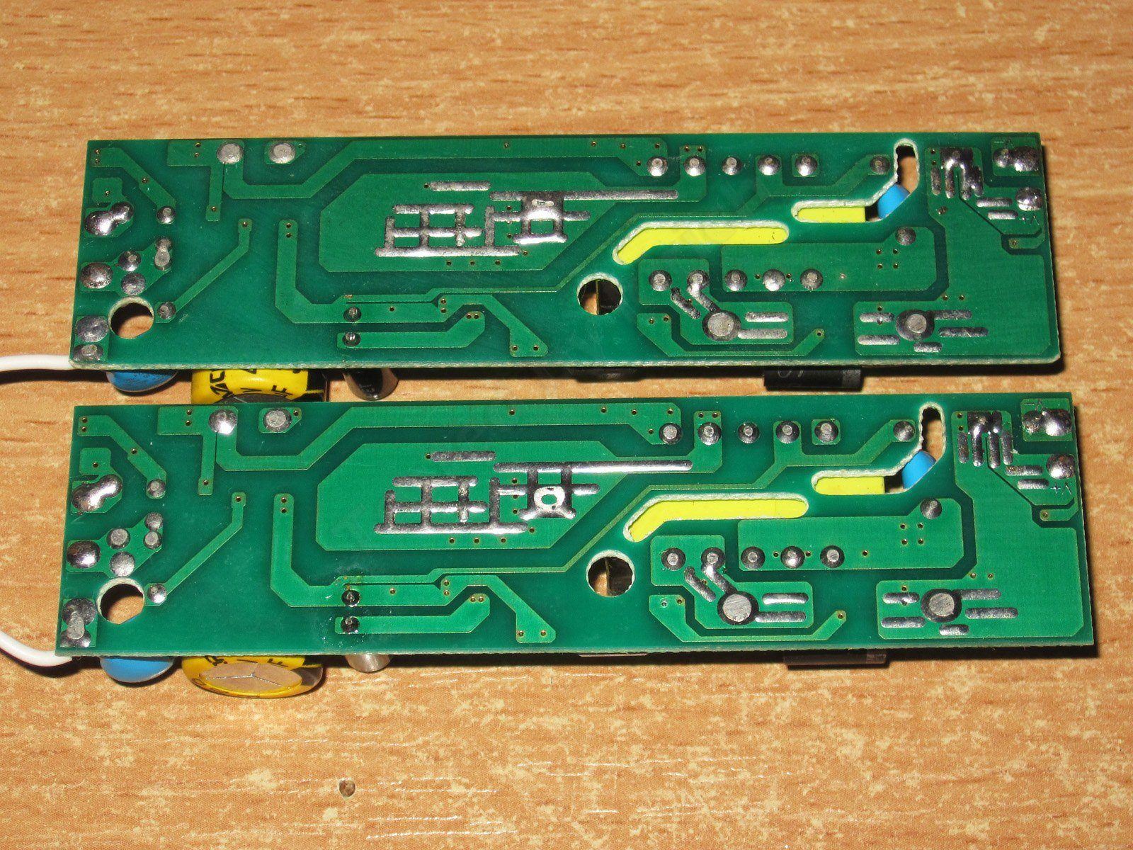
1. There's no input filter. This is the most basic model in the series, but it does have a varistor.
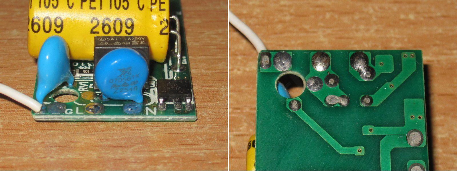
2. The input capacitor is 33 µF.
3. The key difference between the units is the value of one of the shunt resistors.
4. At our request, the manufacturer installed more reliable capacitors, marked Rubycon, though I can't vouch for them.
5. There's a proper capacitor between the primary and secondary sides.
6. At our request, the standard output capacitors were replaced with polymer ones.
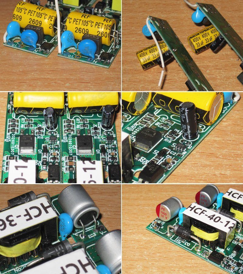
No issues with electrical safety.
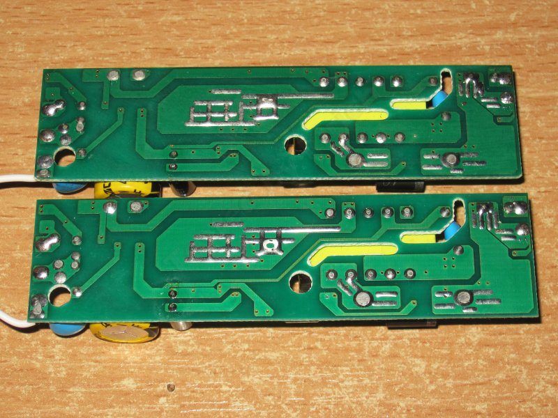
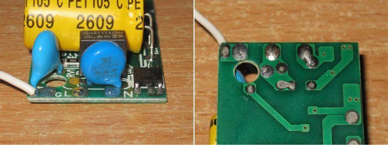
But the varistor issue definitely needs fixing: you mustn't connect a varistor across the input before the fuse.
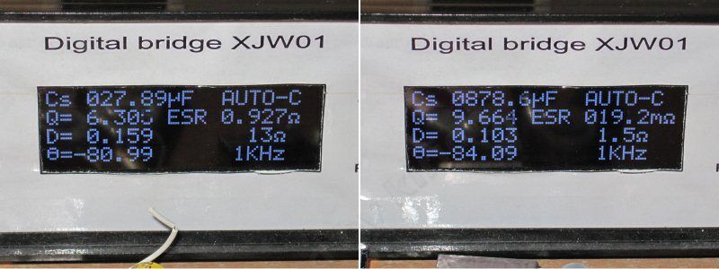
The actual input capacitance is about 28 µF. That's fine for a 230 V mains supply, but too low for 115 V. With a low input voltage, you should either not load it to 100% or expect problems.
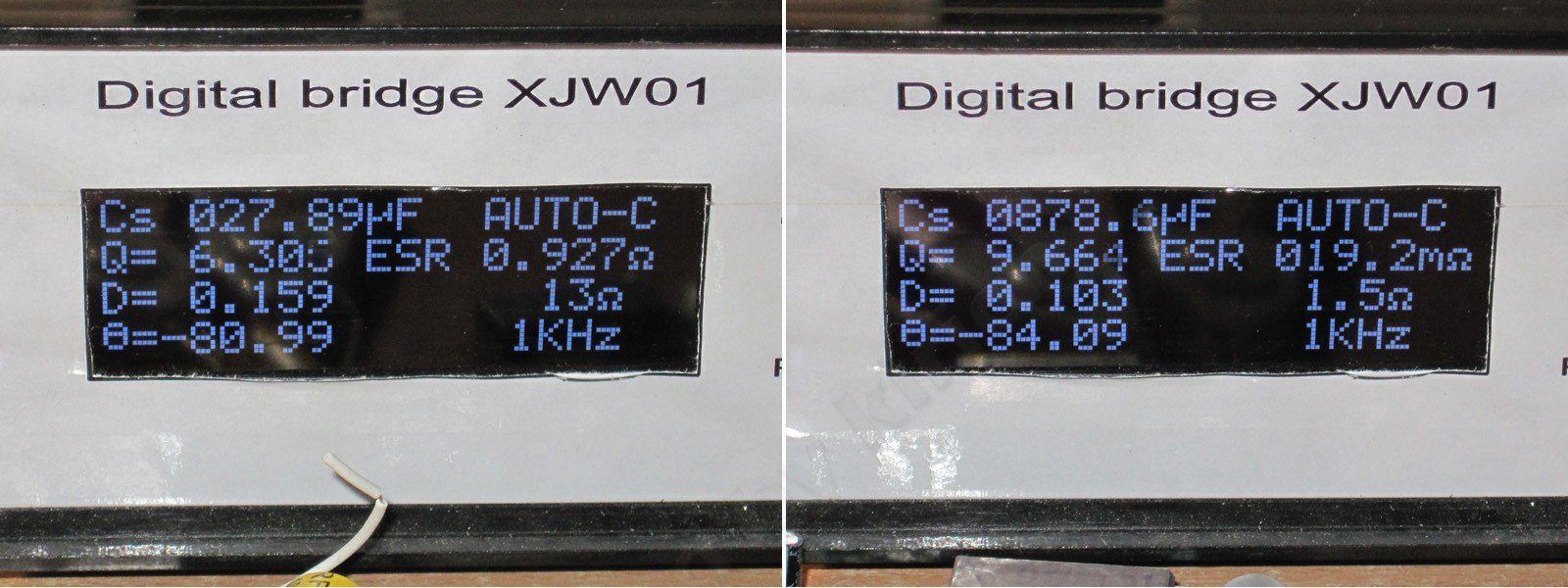
The output capacitance is 880 µF. Since these are polymer capacitors, that's definitely better than before.
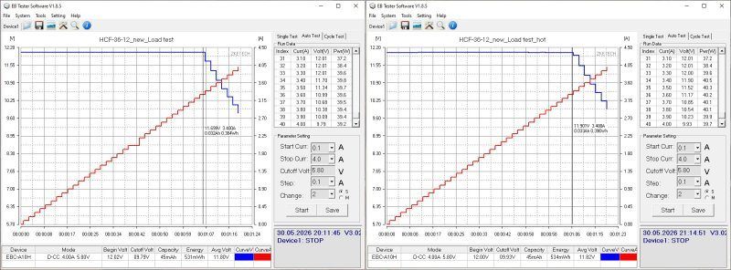
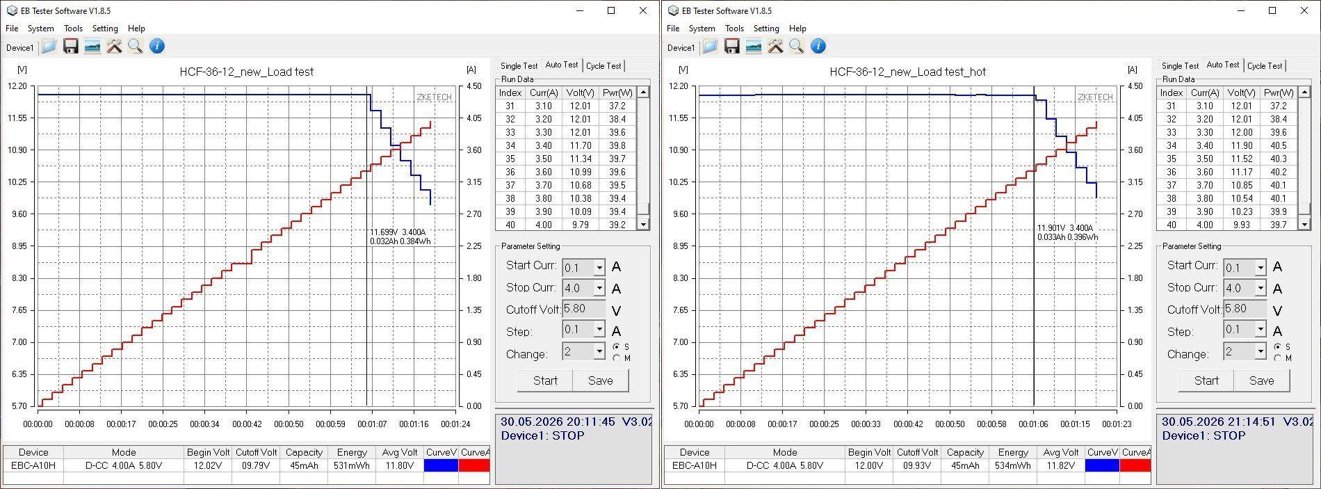
The protection current is set to 3.1 A; beyond that, the power supply starts reducing the voltage. Everything looks fine here. The protection current does not depend on temperature.
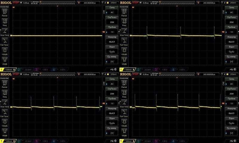
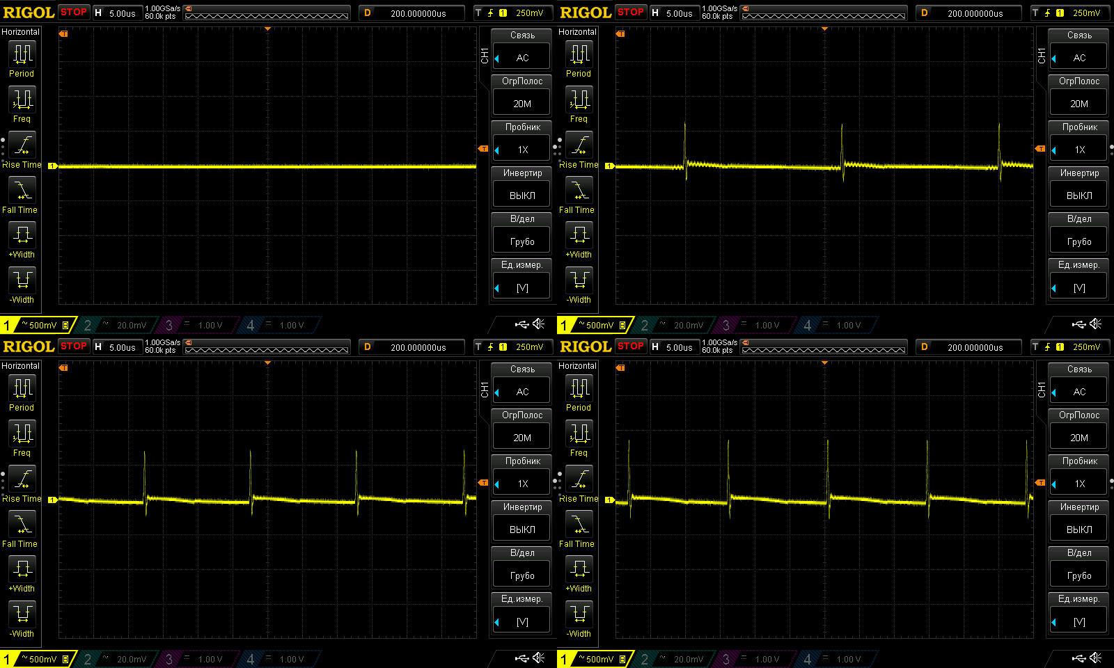
Ripple with no load and at currents of 1, 2, and 3 A.
I have no complaints about the main part of the waveform, but the “spikes” are a bit too large. Several things could be causing them: the snubber, the PCB layout, or even the fact that the output capacitor is lying flat rather than being soldered upright. The last explanation is quite plausible.
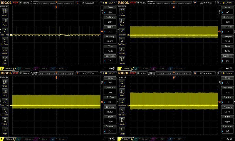
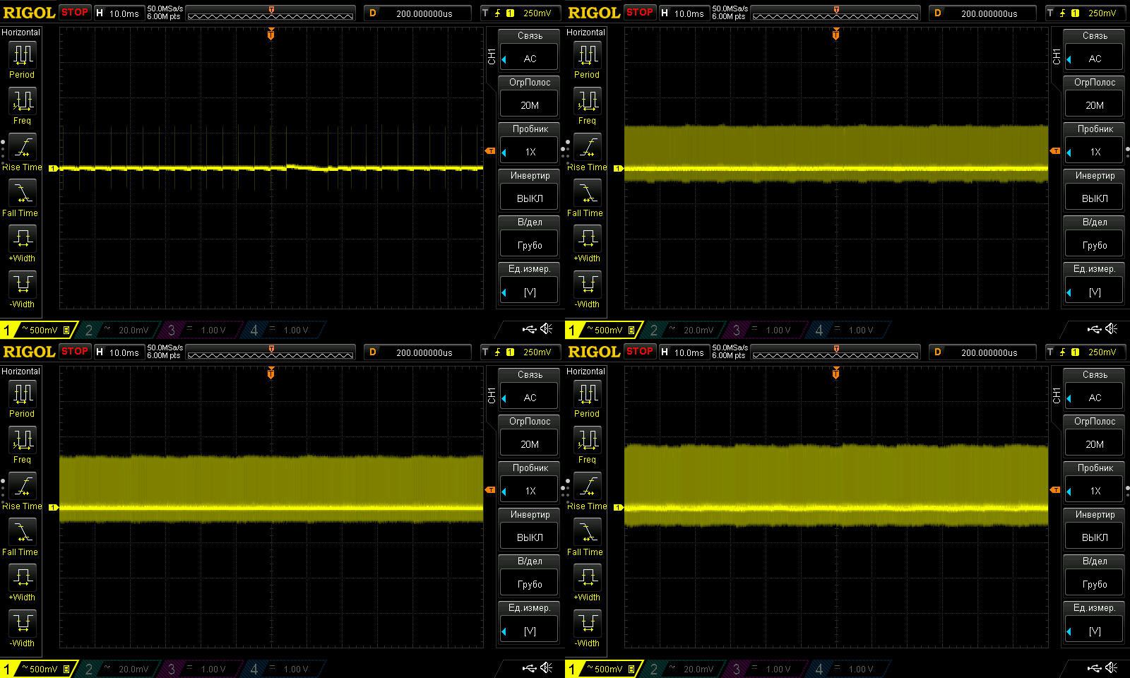
At low frequencies, the main component is actually caused by the “spikes,” which makes the waveform look rather poor.
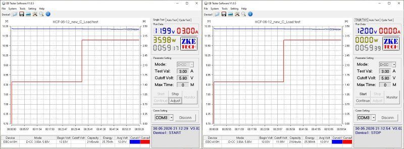
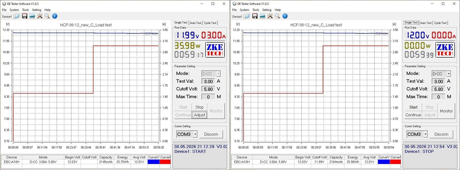
I ran the thermal test at 50% and 100% power for about half an hour each. The output voltage is practically unaffected by temperature.
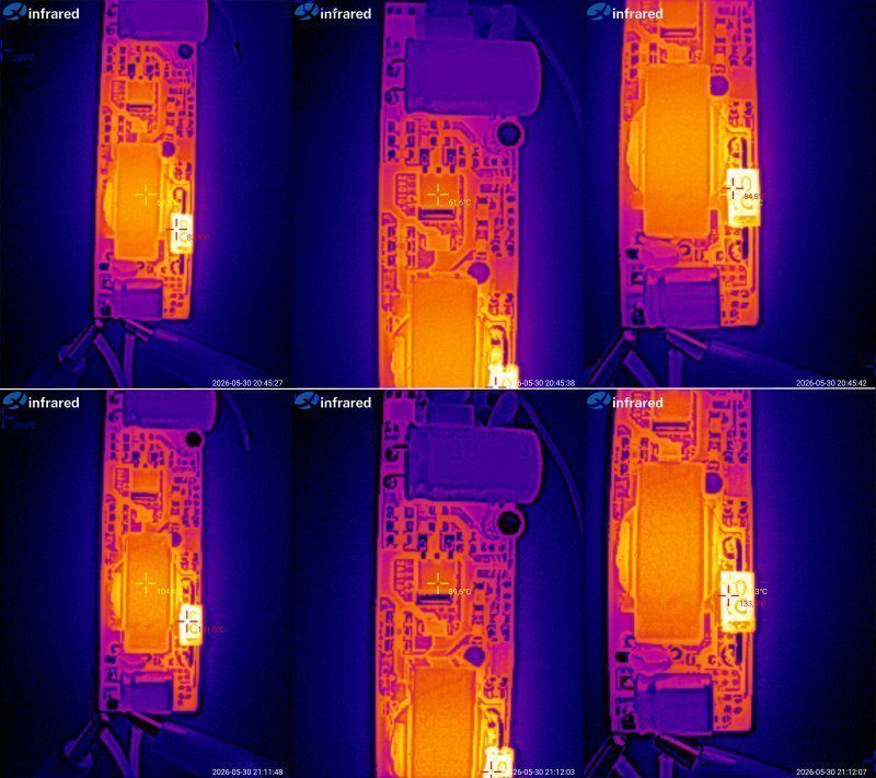
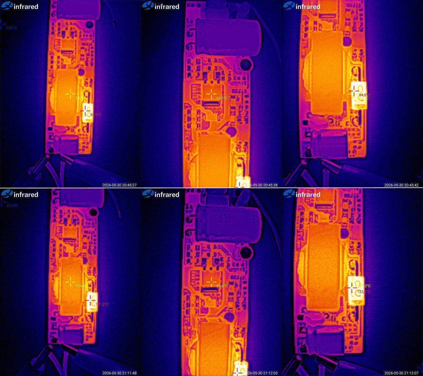
At 1.5 A, the transformer reached 69 degrees, the transistor 62, and the output diode 85.
At 3 A, the transformer reached 104 degrees, the transistor 90, and the output diode 133.
That’s quite a lot, but bear in mind that the power supply isn’t potted in compound, which also helps distribute heat. Incidentally, the 40 W power supply will run at an even higher temperature.
Also bear in mind that I’m testing it at 100% power, although continuous operation at full power is generally not recommended.
60 W power supply, 12 V, 5 A - link
This is where the difference starts to show between the power supplies I tested earlier and the one I’m showing today.
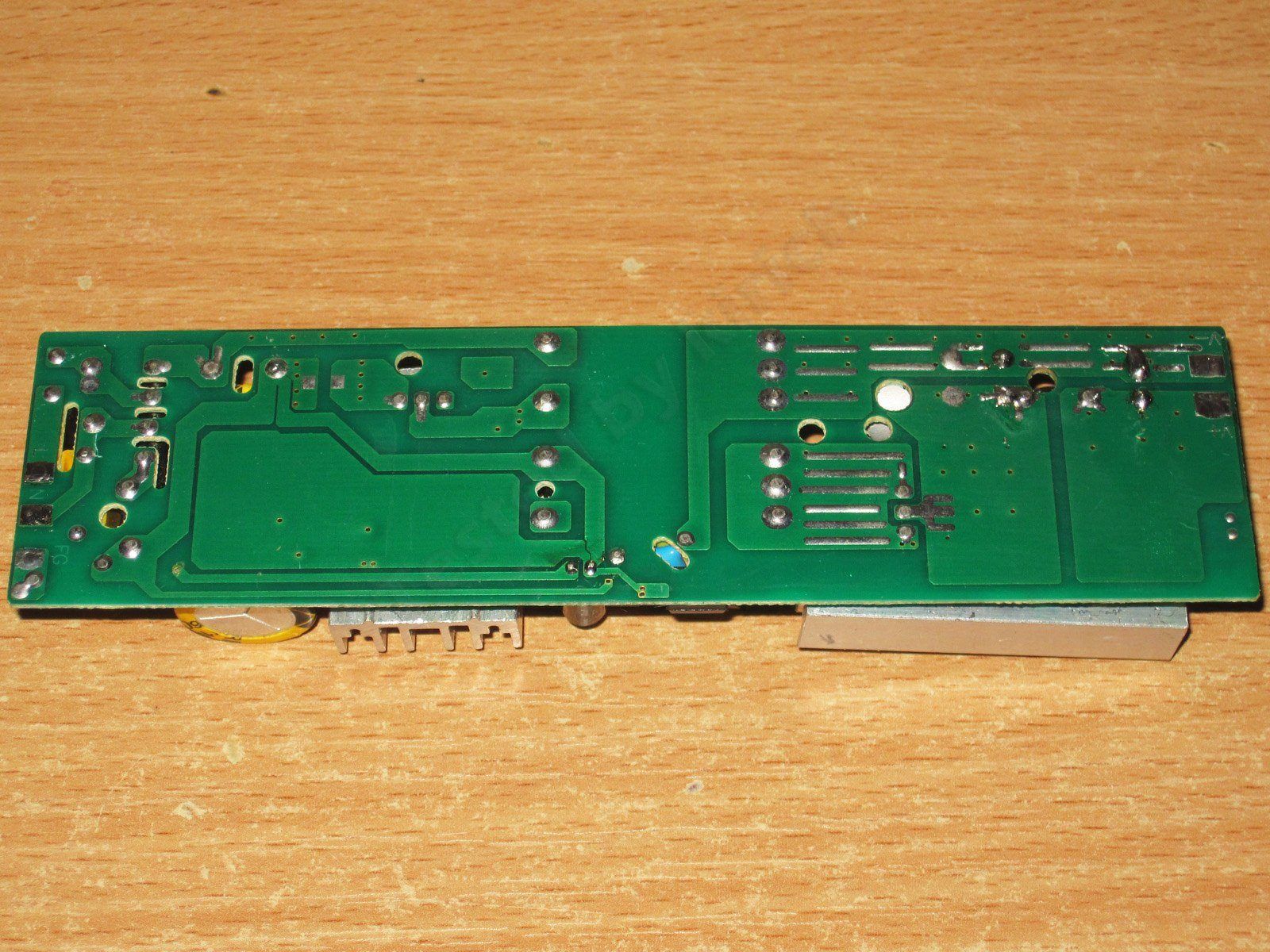
The thing is, the boards I received back then were bare, and I used my own heatsinks. This one has the original heatsinks, so we can see how the cooling is implemented under the potting compound.
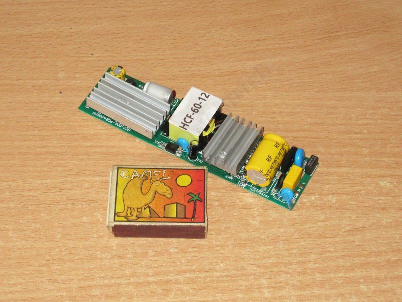
The high-voltage transistor and output diode assembly are cooled by heatsinks. Of course, they’ll behave differently when potted, but the basic point remains: even through the potting compound, heat will be dissipated better than with a diode mounted directly on the board, as in the 36 W and 40 W versions.
Though it’s quite possible that heat will be dissipated even better this way than in open air.
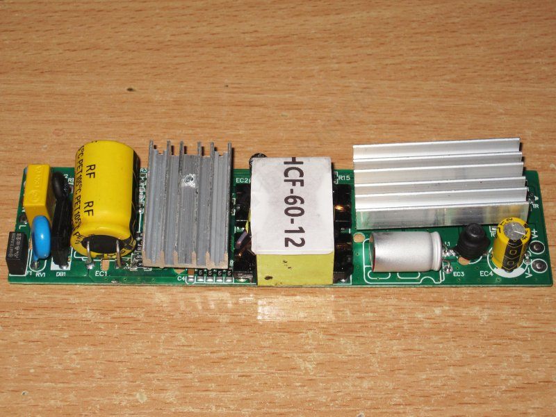
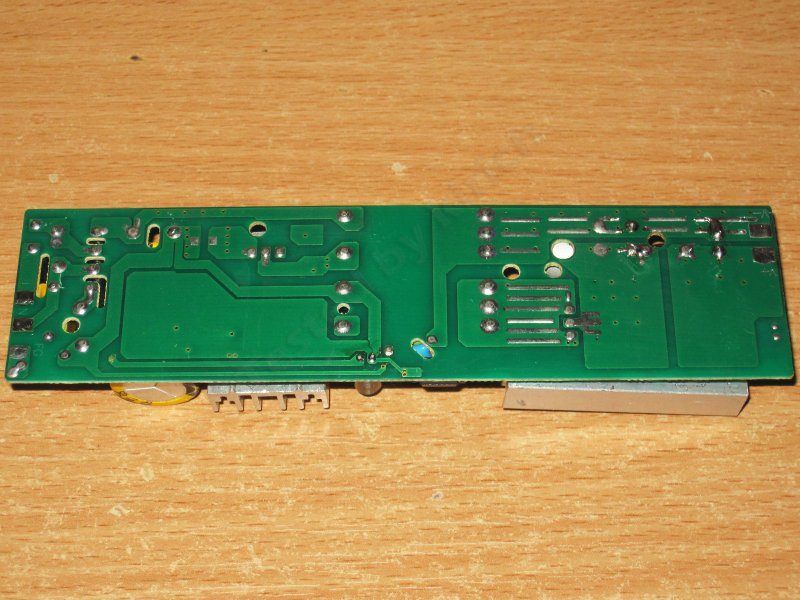
There’s no input filter here, and none is even provided for, but all the other necessary components are present, including a varistor and thermistor. The varistor is also installed correctly here, after the fuse.
The input capacitor is 68 µF.
The shunt resistors made me laugh. I understand this is a prototype, but they look pretty funny :)
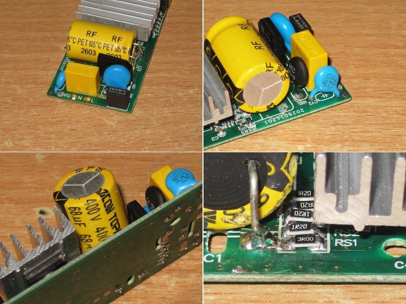
The Y capacitor and the PWM controller’s supply capacitor are also marked Rubycon.
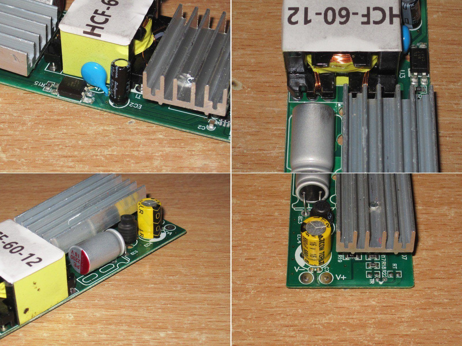
The output winding uses several wires.
The output stage is better here: first, there’s a 2200 µF polymer capacitor; second, there’s an inductor after it, followed by a regular 680 µF capacitor. Replacing the regular capacitor with a polymer one was our requirement.
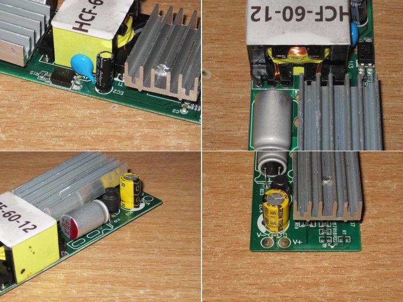
No safety concerns.
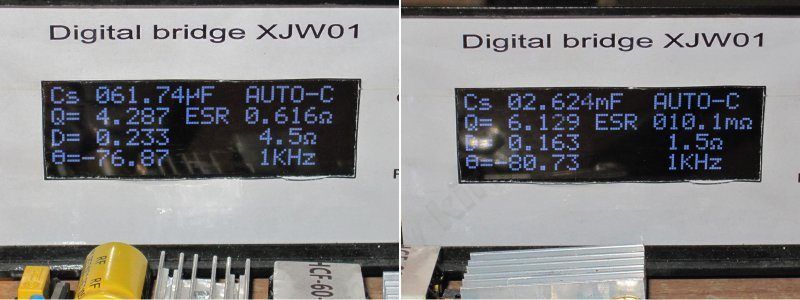
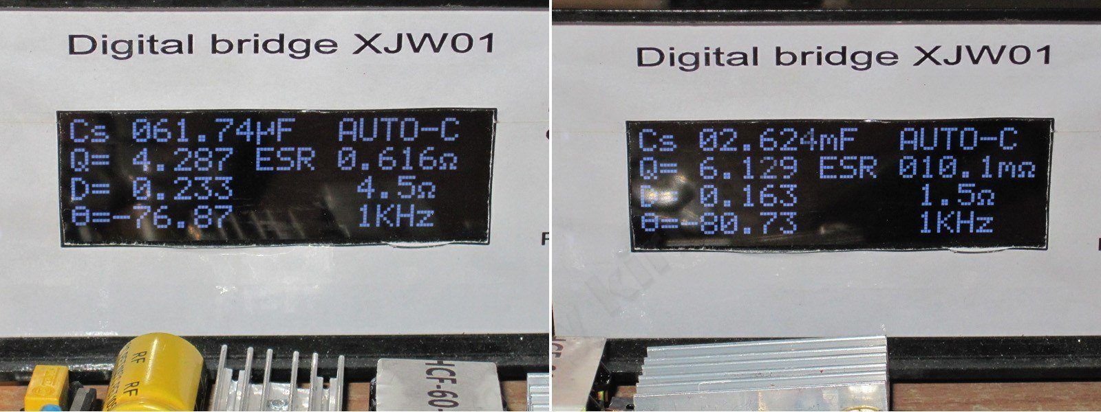
The input capacitor’s actual capacitance is about 62 µF, and the output capacitors total 2600 µF. That’s perfectly fine for a 230 V mains supply; at 115 V, it’s better to reduce the load below the maximum.
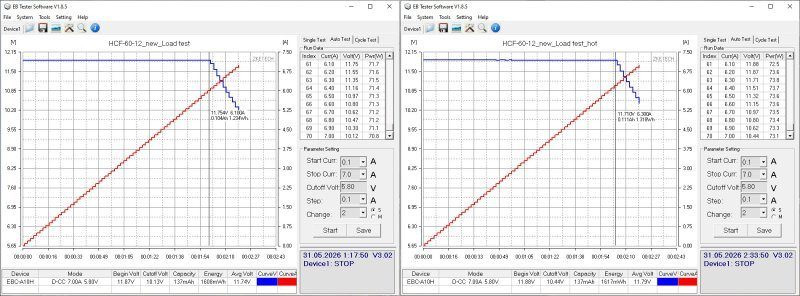
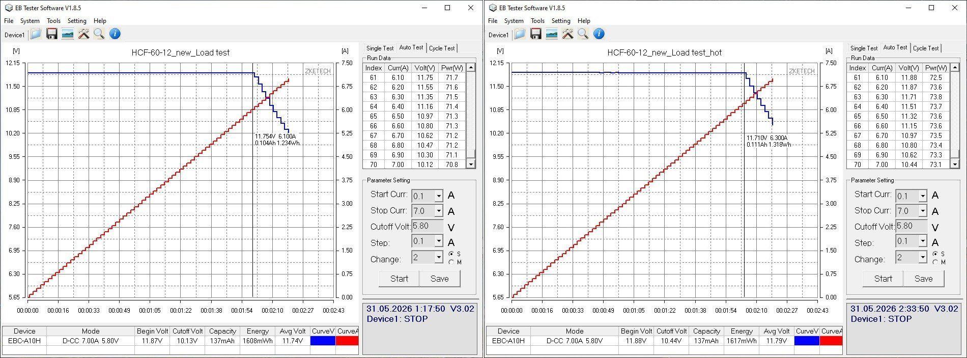
The protection is set to trip at 6.1–6.3 A, both cold and hot. Excellent, in my opinion.
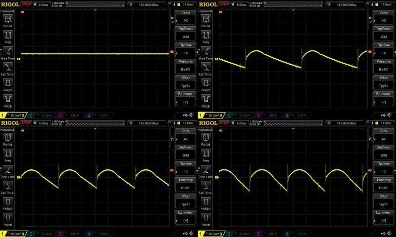
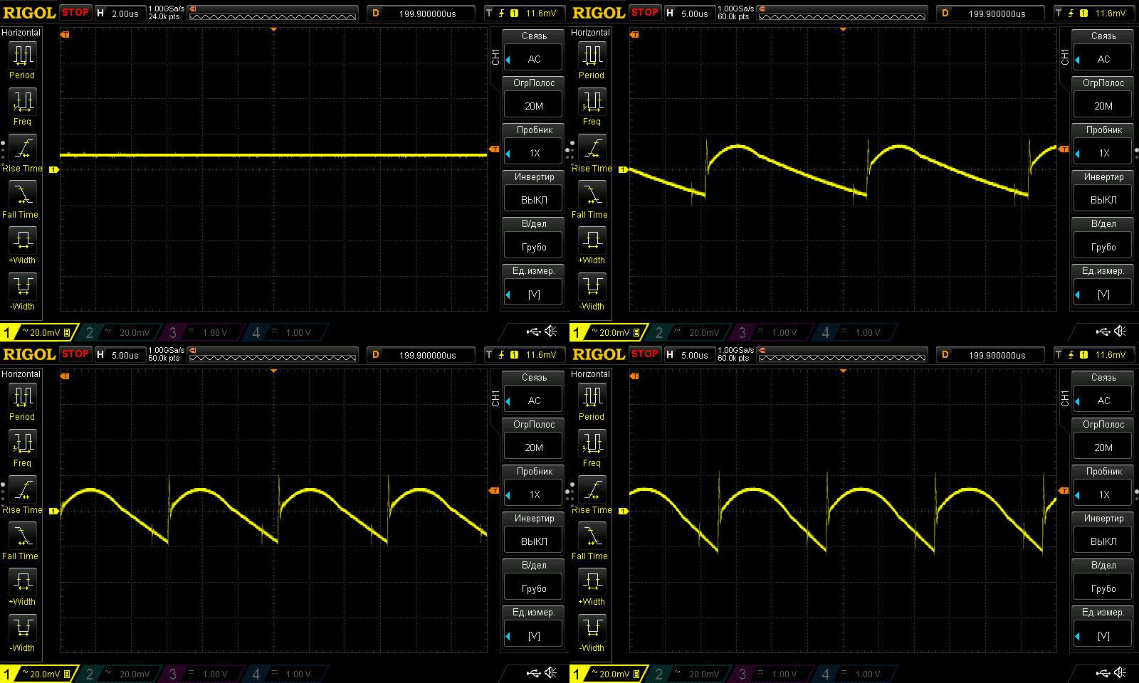
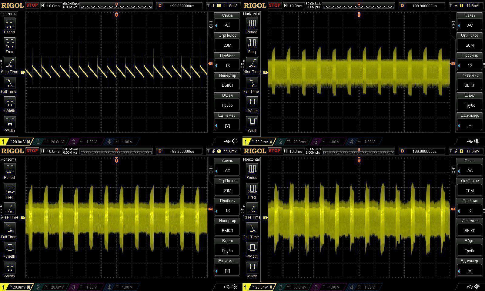
Ripple with no load and at currents of 2, 4, and 5.5 A.
I think 40 mV even at maximum load is pretty good.
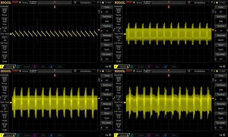
There’s some strange 100 Hz ripple at low frequencies. I’ve written before that it may be a quirk of the PWM controller used here. In this case, though, it’s not particularly critical because the ripple’s peak-to-peak amplitude is small.
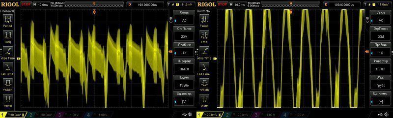
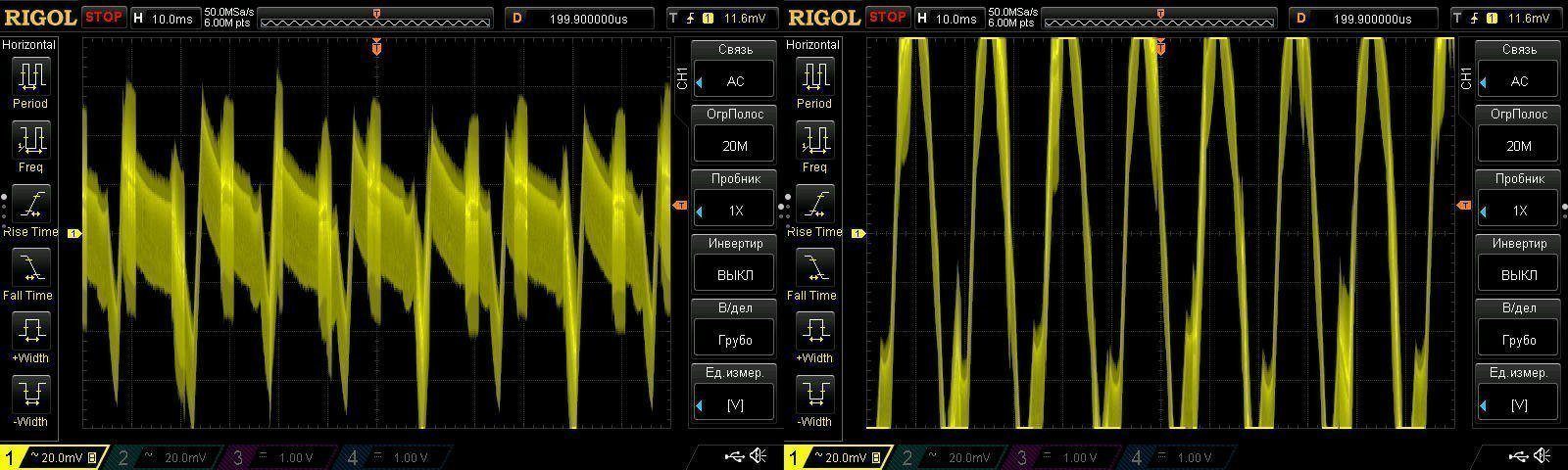
This is a feature of the overload protection. You saw that when the threshold is reached, the PWM controller reduces the voltage rather than shutting off the load.
I don’t recommend pushing the power supply into this operating mode.
On the left, low-frequency ripple at 5.9 A; on the right, at 6 A. You can see that when the power supply starts entering protection, it goes haywire.
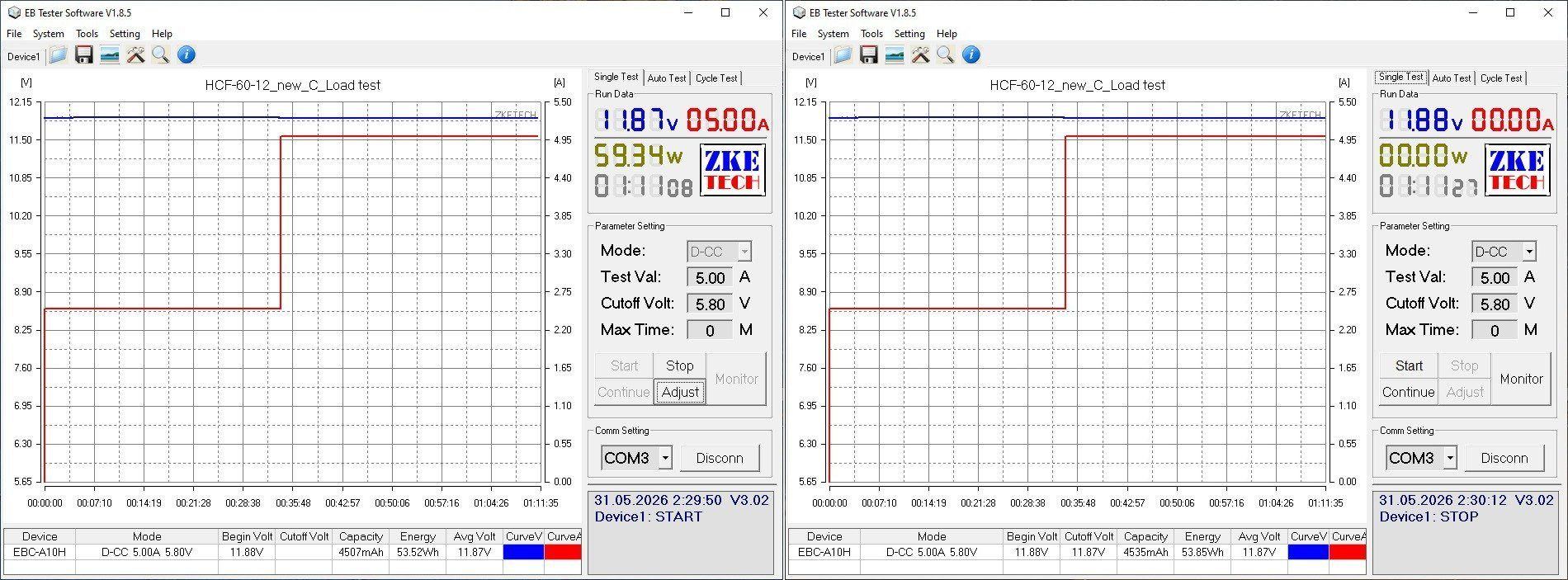
The thermal test was done in two stages, at 2.5 A and 5 A, for a total of over an hour. The voltage is practically unaffected by temperature or load.
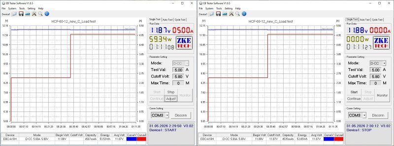
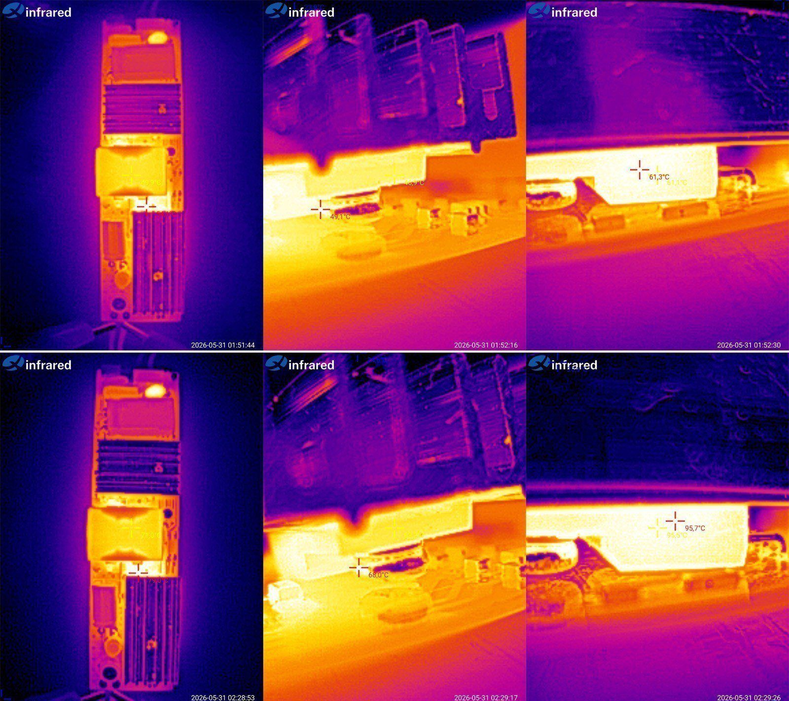
At 2.5 A, the transformer reaches 50 degrees, the transistor 49, and the diode assembly 61.
At 5 A, the transformer reaches 71 degrees, the transistor 68, and the diode assembly 96.
As you can see, in this configuration the power supply has a decent amount of headroom—at least 20–25 degrees. Potting it will change things a little, but I don't think it will change much; and besides, it's hard to say which way things will go. I'd expect it to be better.
HCF-100-12 power supply: 100 W, 12 V, 8.3 A — link
This one is even closer to the real-world setup. The only difference from the finished version is that it hasn't been potted. The power supply is still in its original enclosure, which acts as a heatsink. And of course, this affects the final component temperatures. It's fairly difficult to predict exactly how, since the potting compound doesn't cool anything; it just spreads (equalizes) the heat across the enclosure. So some components will fare better, and others worse.
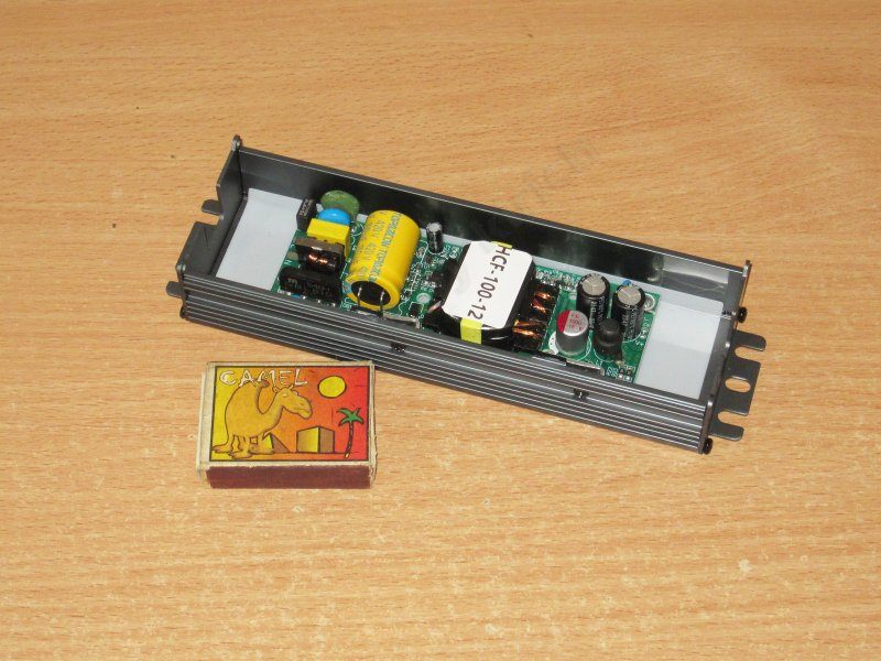
The board is noticeably smaller than the enclosure, so I think it should cool even better once potted.
I have no complaints about the build quality, and for some reason I just like this power supply.
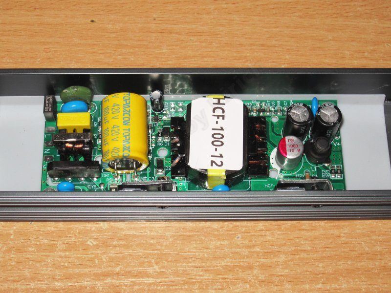
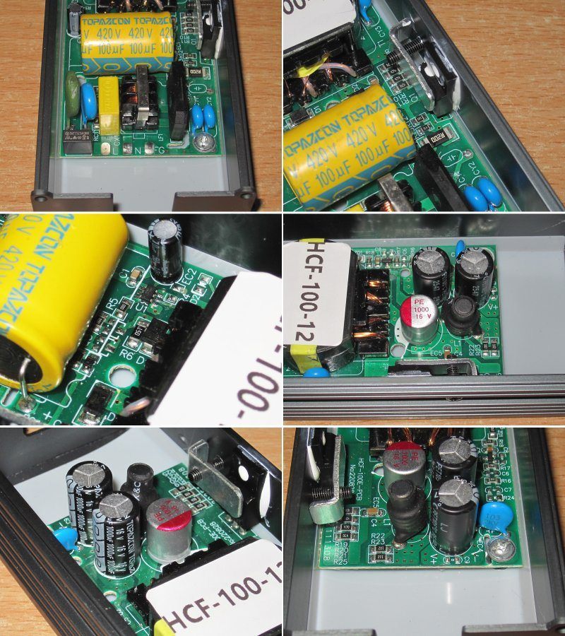
1. The input already has a proper filter, as well as a varistor, thermistor, and several Y capacitors.
2. As expected, the transistor is mounted with thermal paste. A 200 mΩ shunt is visible nearby.
3. PWM controller. There's a spot nearby for the MOSFET driver transistors, but they're not used in this version.
4. The output has two standard capacitors and one polymer capacitor, plus an inductor to reduce ripple. The inductor is clearly rated for a fairly high current.
5. All the capacitors are 1000 µF, and the diode assembly is also mounted with thermal paste.
6. One thing that surprised me when I started checking it: there are no contact pads for connecting the output cable. So I soldered it to the spot where the output ceramic capacitor was supposed to go :)
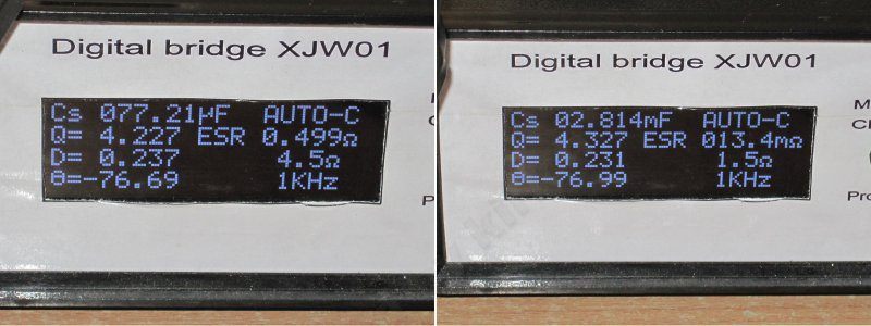
The actual input capacitor capacitance turned out to be noticeably lower than specified: it's rated at 100 µF, but measures about 77. At the usual 230 V, this isn't particularly critical, of course—it'll work just fine—but it's a little disappointing.
The output is closer to spec: 2800 µF, ESR 13.4 mΩ. No complaints there.
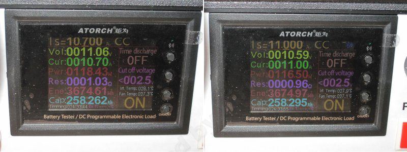
When I tried to determine the protection trip current, I hit the limit of my electronic load, which is 10 A, both cold and hot.
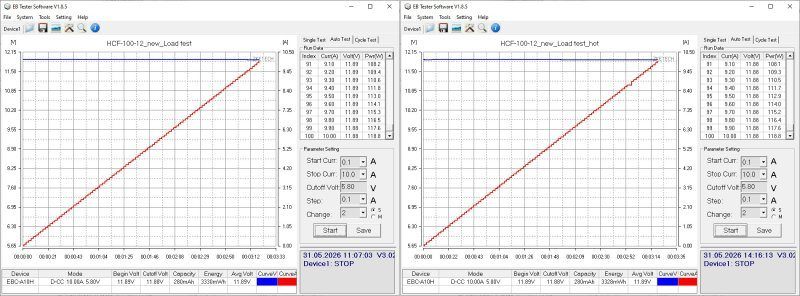
The test showed, first, that the protection is set to about 10.5 A, and second, that the power supply reduces its voltage as the load increases—in effect, it switches to a mode close to constant-power regulation.
This is a little debatable. I might have used a 220 mΩ shunt instead of 200 mΩ, which would bring the protection current down by about 10%, but overall it's not critical.
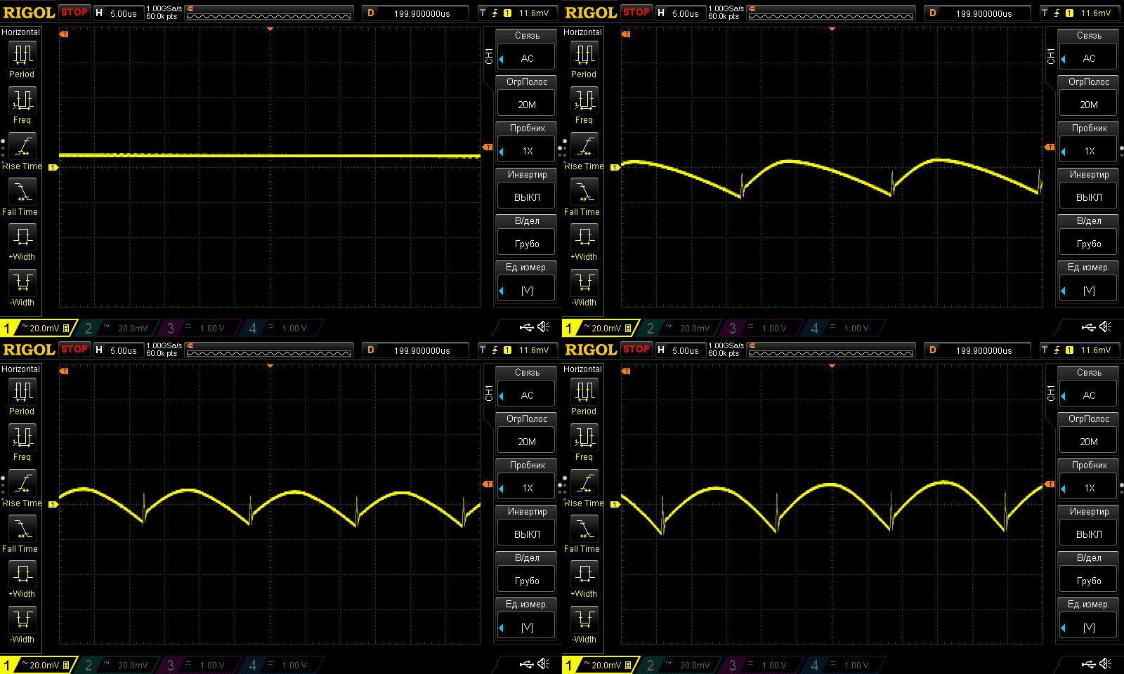
Ripple at no load and at 3, 6, and 9 A looks excellent here too: just 30 mV even at the heaviest load, and essentially no "spikes".
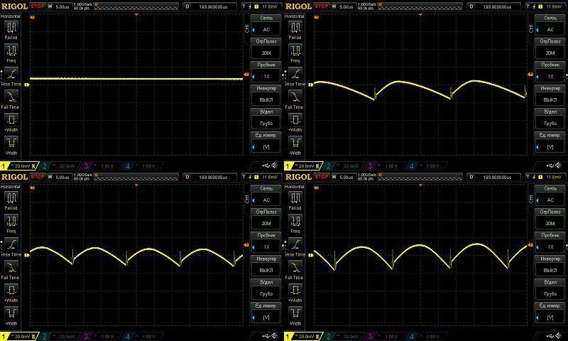
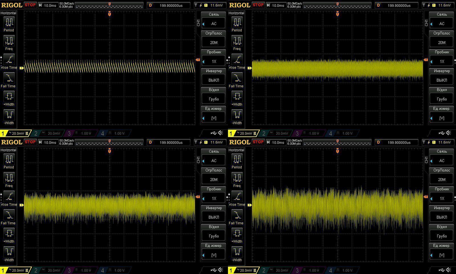
Ripple at the mains frequency is also fine, and given the overall level, it's excellent.
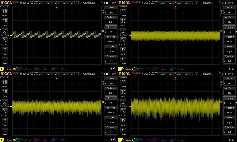
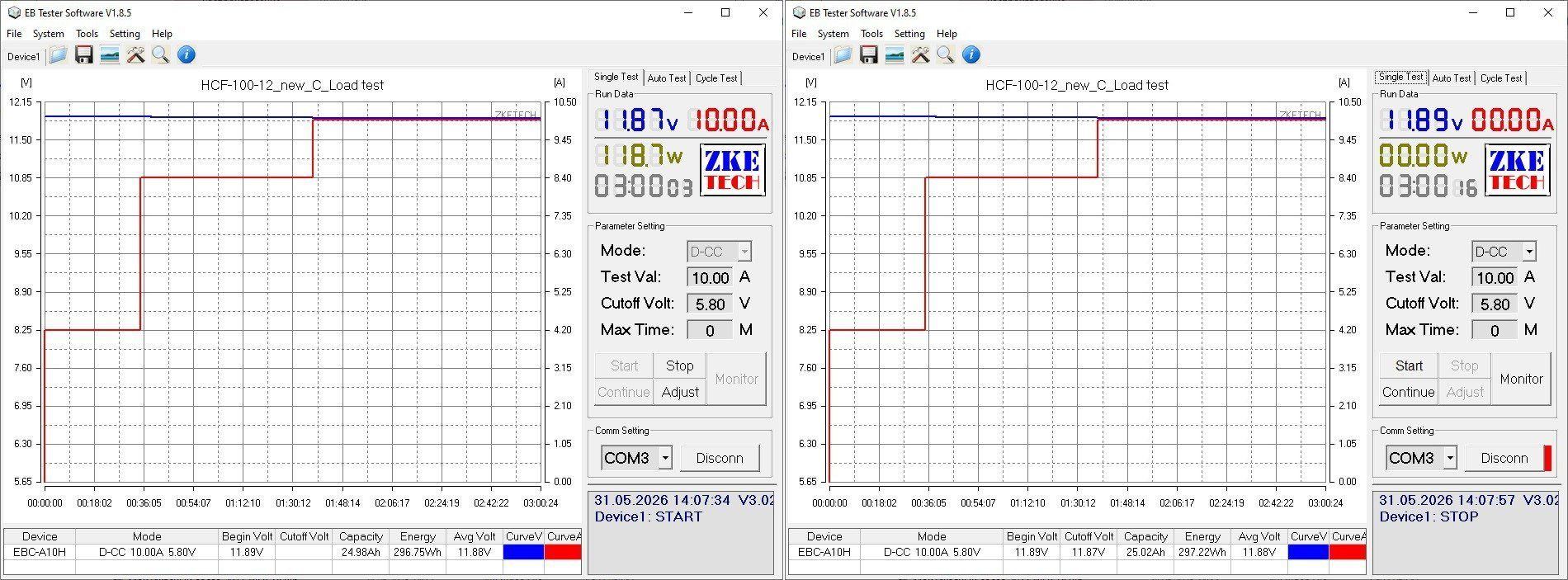
The temperature test was run at 4.2 and 8.4 A, roughly 50% and 100% load. Then I added another stage at 10 A, i.e. 20% above the maximum.
The voltage varies slightly with the load, by just 20 mV, and shows no noticeable dependence on temperature.
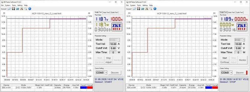
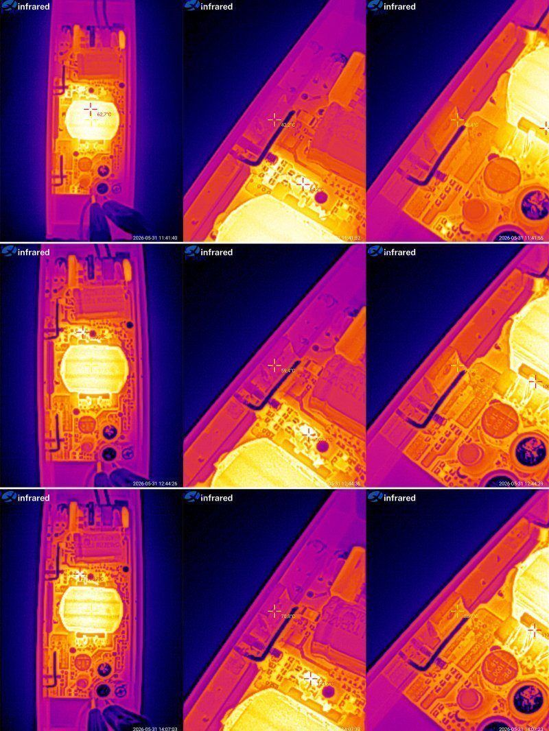
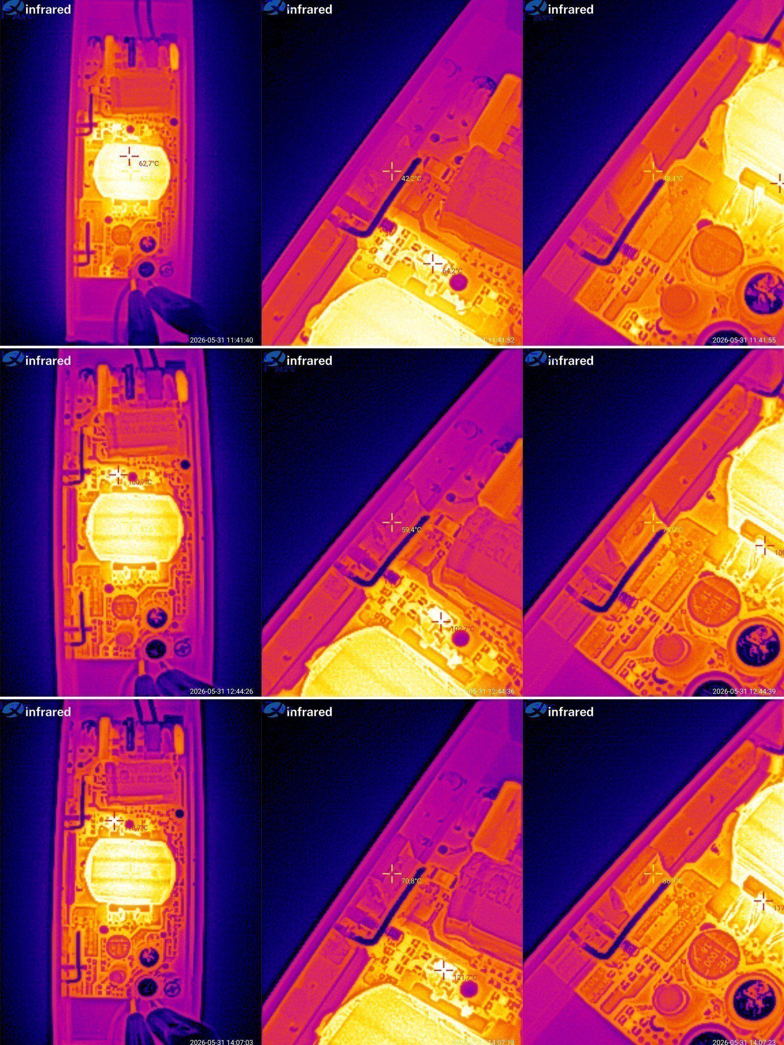
And here are the results.
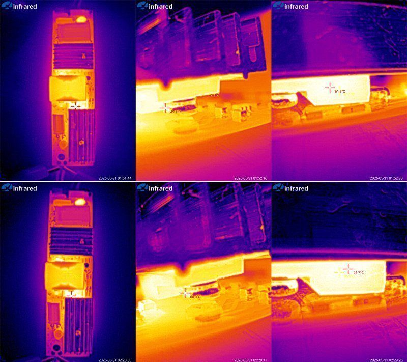
4.2 A — transformer at 63 degrees, transistor at 42, diode assembly at 48
8.4 A — transformer at 98 degrees, transistor at 59, diode assembly at 75.
10 A — transformer at 115 degrees, transistor at 71, diode assembly at 87.
The only real concern is the transformer temperature. But keep in mind that once it’s potted, the heat will be distributed more evenly, so the temperature will probably drop a little. It should be able to deliver its rated 100 W continuously without any problems.
Model HCF-150-12, 12 V, 150 W, 12.5 A — link.
This model is very similar to the previous one, but scaled up for higher power.
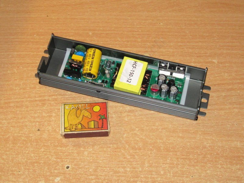
The layout is practically unchanged, with a few minor tweaks. Basically, they took the 100 W power supply, replaced the key components with higher-power ones, increased the capacitor capacity, added another diode assembly, and ended up with a 150 W power supply.
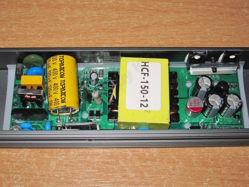
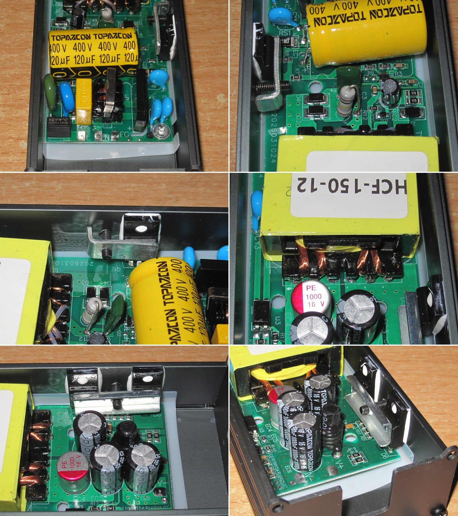
1. It also has an input filter, varistor, thermistor, etc. The input capacitor is rated at 120 µF.
2. PWM controller section; the snubber components are also visible here.
3. The transistor is held against the heatsink with thermal paste.
4. The transformer winding uses Litz wire—nice.
5. There are two diode assemblies in parallel on the output; I approve.
6. There are four output capacitors: three standard ones and one polymer capacitor, all rated at 1000 µF. There’s also an inductor to reduce ripple.
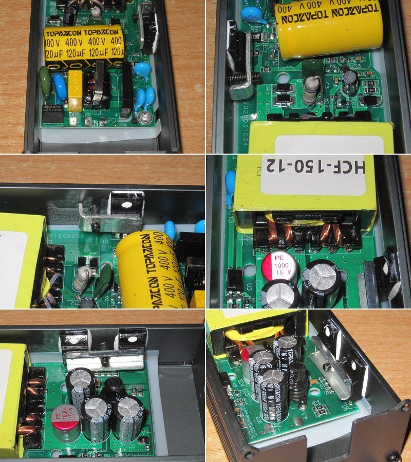
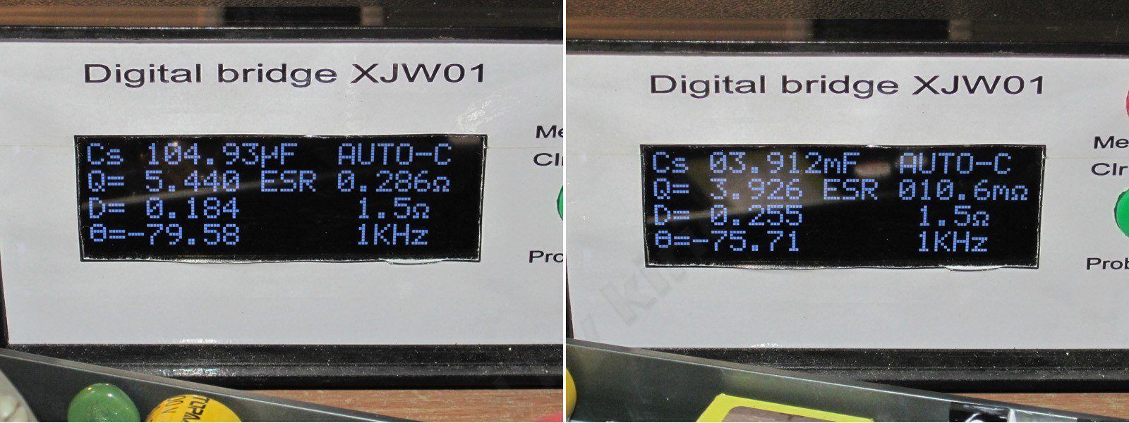
The input capacitor measures about 105 µF, which is acceptable for 230 V, though I’d like to see more; it’s too little for 115 V.
The output capacitance measures about 3900 µF, which is practically what’s specified. ESR is 10.6 mΩ, 30% lower than in the 100 W version. Good.
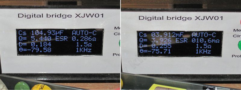
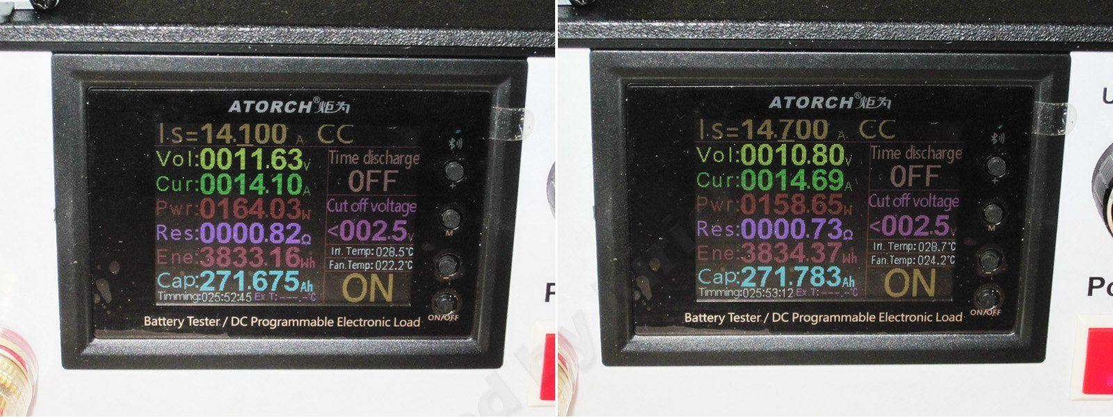
It looks like the same PWM controller is used, since the power supply behaves the same as the 100 W version when it comes to protection: it doesn’t shut down, but reduces the output voltage. The threshold is set to about 14 A; at 14.7 A, the output is already down to around 10.8 V.
For the rated current of 12.5 A, I’d lower it a little, but overall it’s perfectly fine as is and can be left alone.
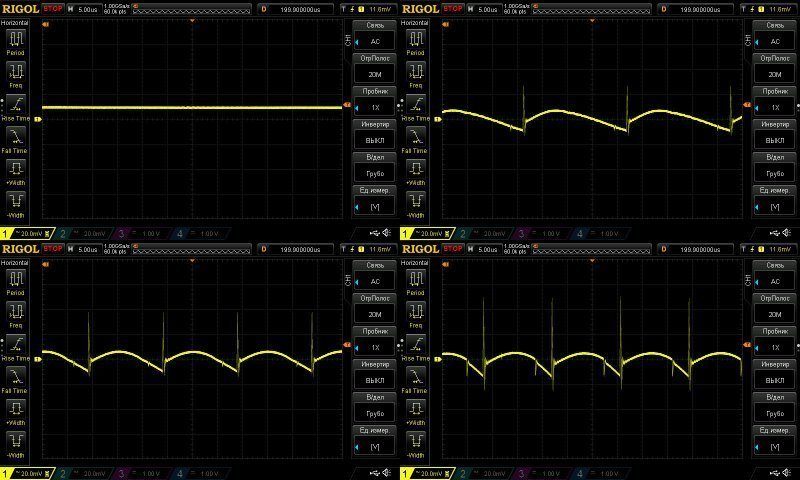
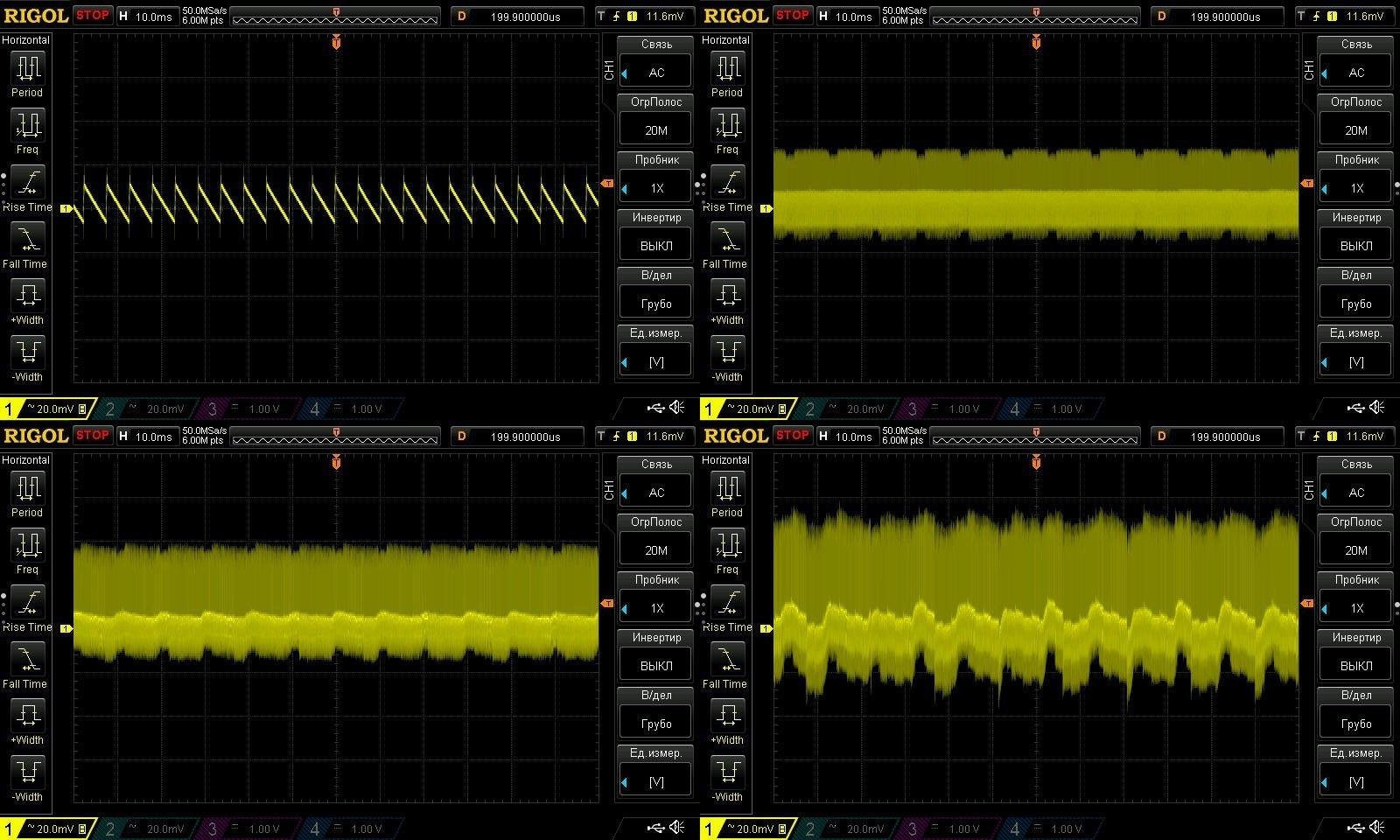
Ripple with no load and at currents of 4, 8, and 13 A.
The main part is practically unchanged: we get about the same 30 mV as with the 100 W version, which is good. But there are now “spikes.” They’re not critical, and the overall amplitude is small. Still, something tells me that in this case, as well as based on measurements of the previous model, this may be a quirk of the circuit board layout.
In any case, the overall verdict is very good.
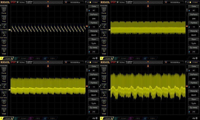
At low frequency, the waveform is predictably worse than on the 100 W version. But even here, the total amplitude is only around 60 mV, so I have no complaints.
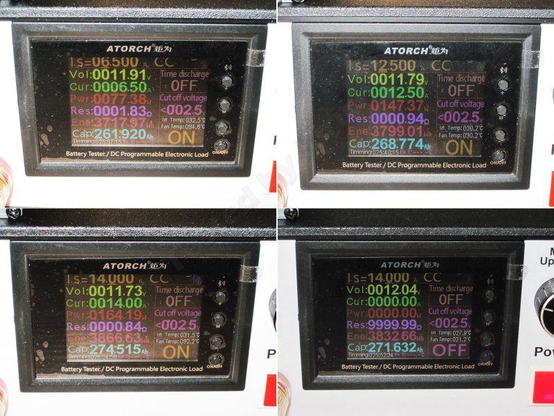
The temperature test was run in three modes: the rated 6.5 and 12.5 A, plus an additional test at 14 A, i.e. at the maximum protection setting.
The first two stages lasted about 25–30 minutes each, and the third ran longer, almost 50 minutes, so I consider the test sufficient.
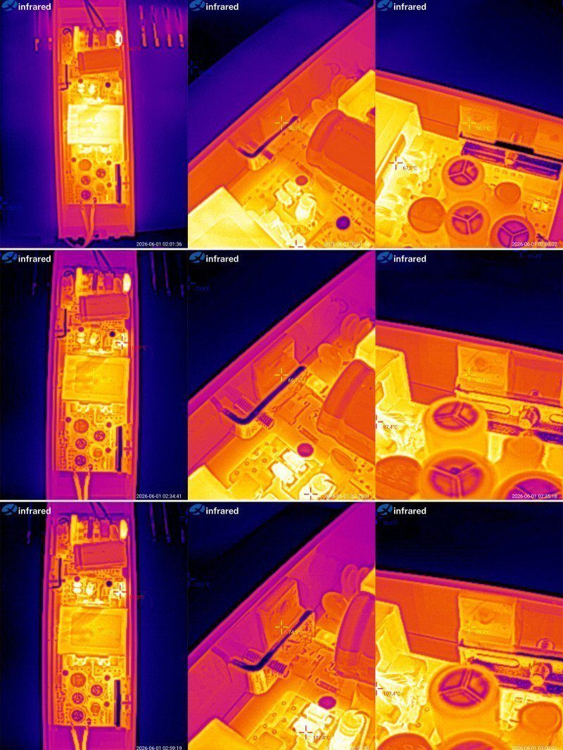
Results:
6.5 A — transformer 64 degrees, transistor 50, diode assemblies 56
12.5 A — transformer 87 degrees, transistor 66, diode assembly 80
14 A — transformer 94 degrees, transistor 75, diode assemblies 90.
Everything looks excellent here. The power supply has plenty of headroom even at the maximum possible 14 A. It definitely warmed up over 50 minutes, and considering it will be potted, that's even better.
There's no point even discussing the normal 12.5 A operating mode; it still has 20–25 degrees of headroom.
Model HCF-200-12, rated for 12 V, 200 W and about 16.5 A — link
This one is more interesting. Although this power supply is only 50 W more powerful than the previous one, it uses a different topology: a half-bridge, used in higher-power designs.
So 150 W was the upper limit for flyback converters, while this one is at the lower end for half-bridges. It'll be interesting to compare them.
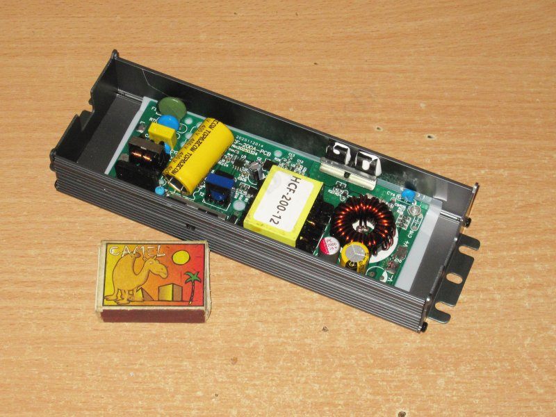
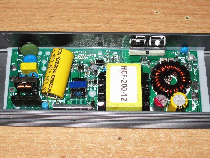
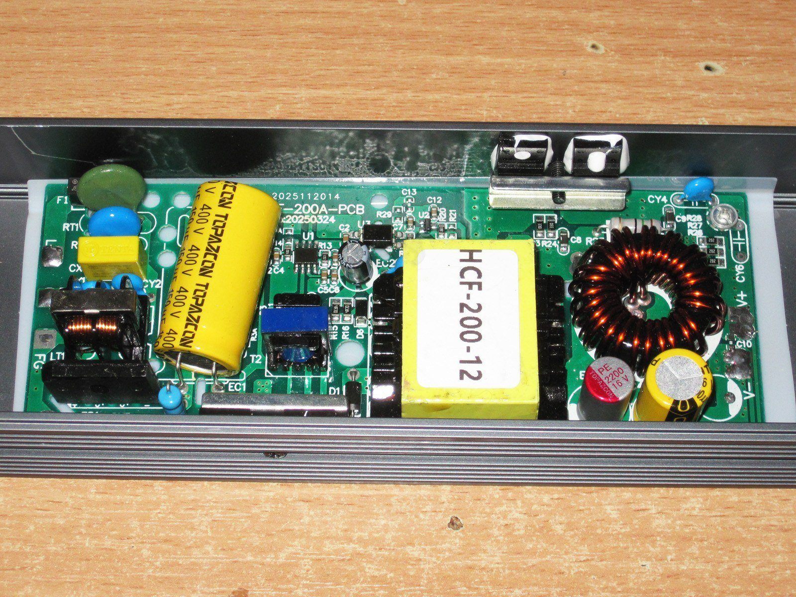
The circuit design is different, and the layout is somewhat similar, but the large output choke stands out immediately, along with the isolation transformer used to drive the transistors.
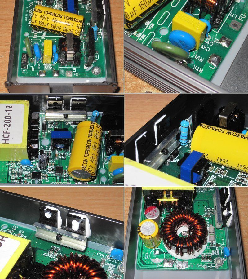
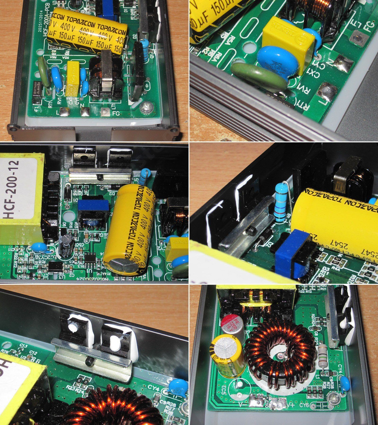
1. A full input filter, with an input capacitor rated at 150 µF.
2. As in all the previous models, there's a 560 V varistor, rated for peak voltage. Its purpose is essentially to protect against short high-voltage spikes.
3. The PWM controller section. You can also see that the transistors are mounted with thermal paste. PWM controller: NCP1252.
4. The current-sense shunt gave me some pause early on, so I asked to have it replaced with a higher-power one.
5. There are two diode assemblies on the output, but unlike the previous models, they aren't connected in parallel; each one is in its own leg.
6. There are two output capacitors, both 2200 µF: one standard, the other polymer. The polymer capacitor is really just there as an extra precaution, since the topology means the capacitors operate under less stress than in the previous models.
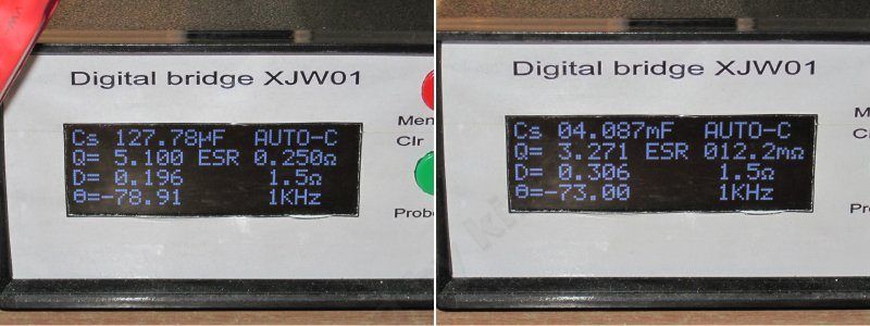
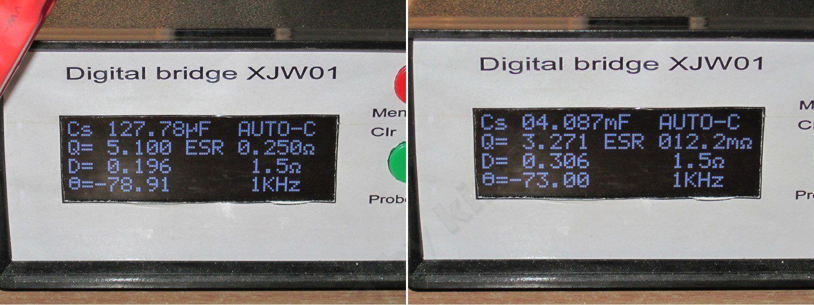
The input capacitor's actual capacitance is 127 µF. That's a little low, but not excessively so. This topology only operates over a narrow range—in this case, 230 V—so it doesn't need a large capacitance. Even Mean Well units have a similar capacitance.
For example, a 200 W Mean Well with the same topology has a 165 µF capacitor. What bothers me more is that it’s rated for 150, which is perfectly reasonable, but in reality it’s 127 :(
The output capacitance is about 4100 µF, which is more than enough for these operating conditions.
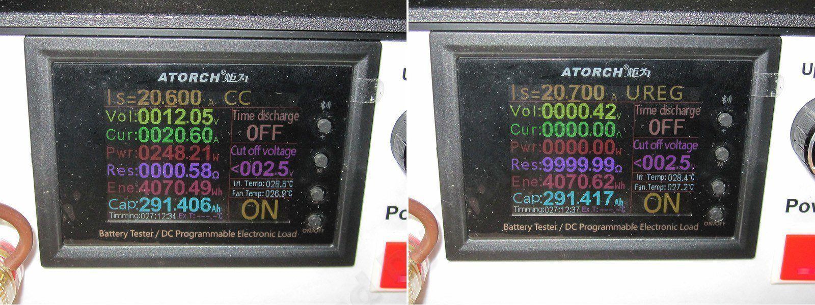
Overload protection completely shuts off the output for a while. The trip current is about 20.7 A.
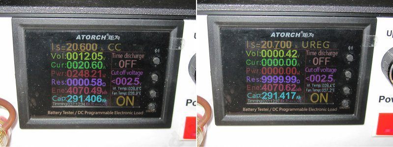
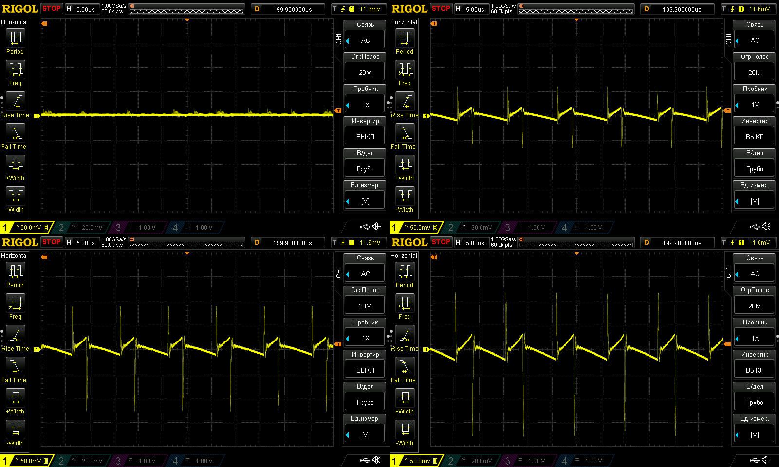
Ripple with no load and at currents of 6, 12, and 18 A.
The main ripple is around 50–60 mV, but there are some pretty pronounced “spikes.” In the vast majority of cases, the load won’t care about them, and most of them will be filtered out by the cable anyway.
But there’s something odd here, because this topology usually has almost no output ripple at all, especially considering that there’s a polymer capacitor on the output. Mean Well doesn’t use polymer capacitors in its LRS200, LRS350, or even more powerful models, though the conventional capacitors it does use are very good.
Overall, my personal opinion is that the PCB layout isn’t quite optimal somewhere.
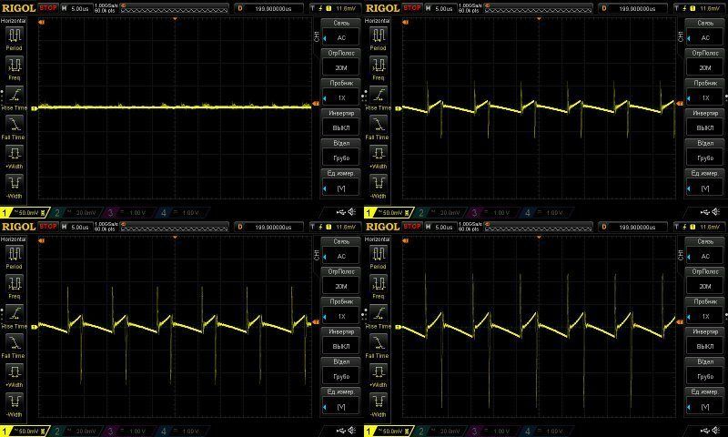
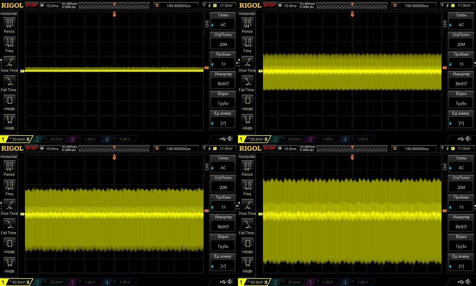
At low frequencies, the total noise amplitude is about 300–350 mV, most likely because of those spikes. But the 100 Hz component is almost absent, which is good.
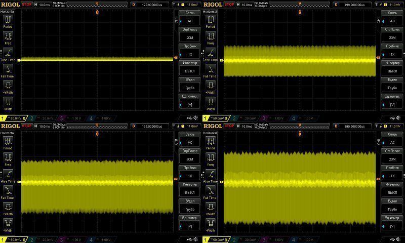
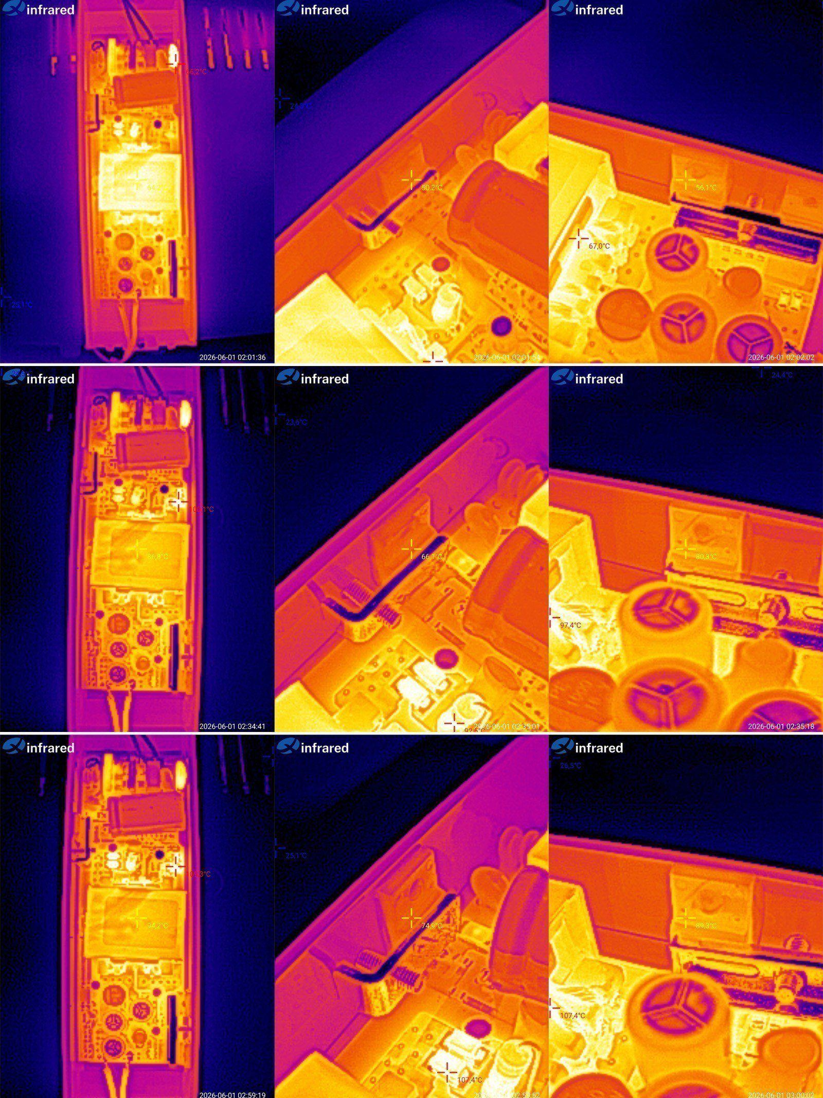
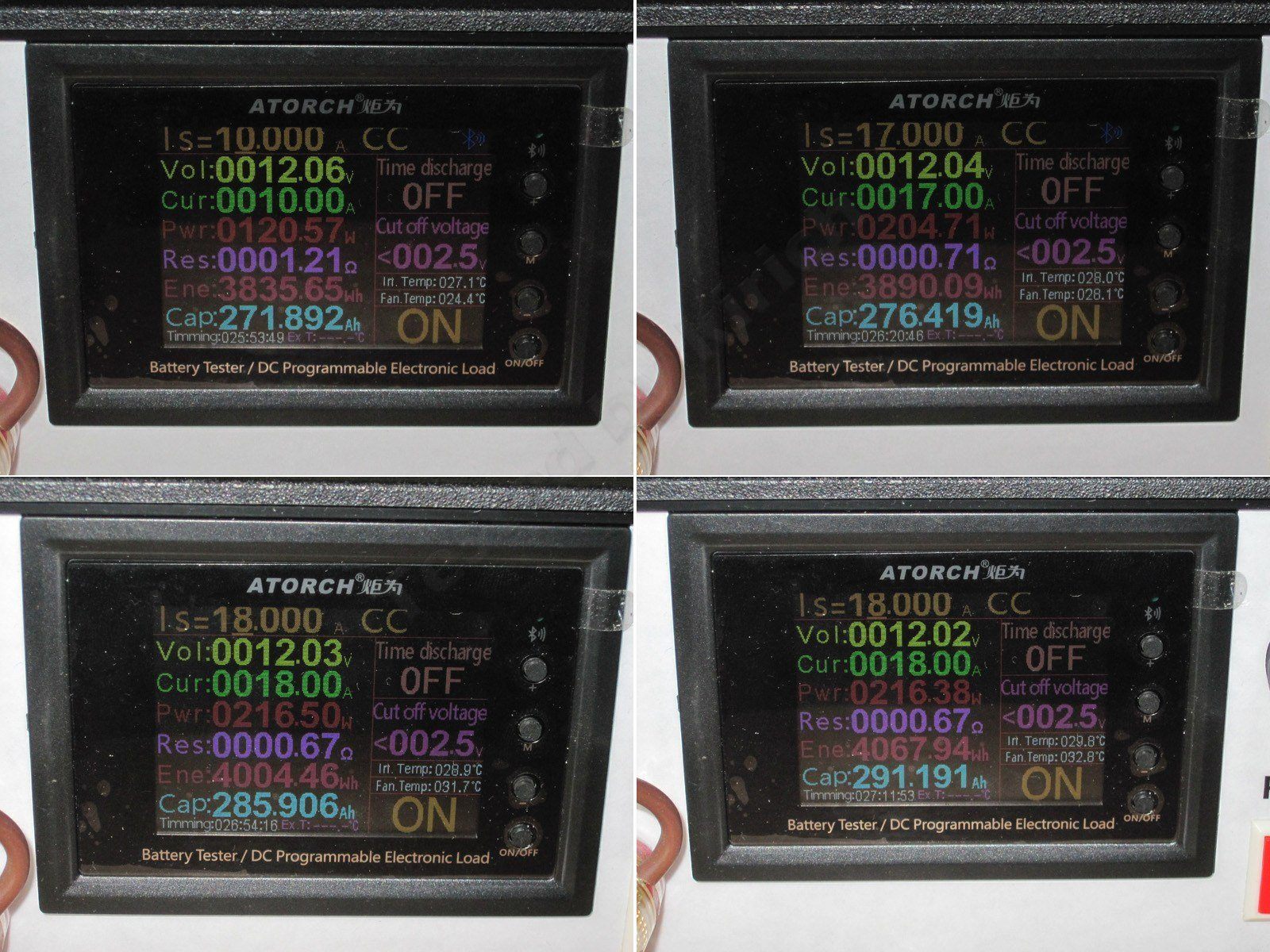
The test was run in three modes: the two main ones, at 10 and 17 A, plus an additional 17-minute run at 18 A.
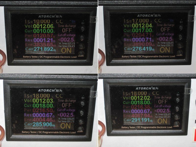
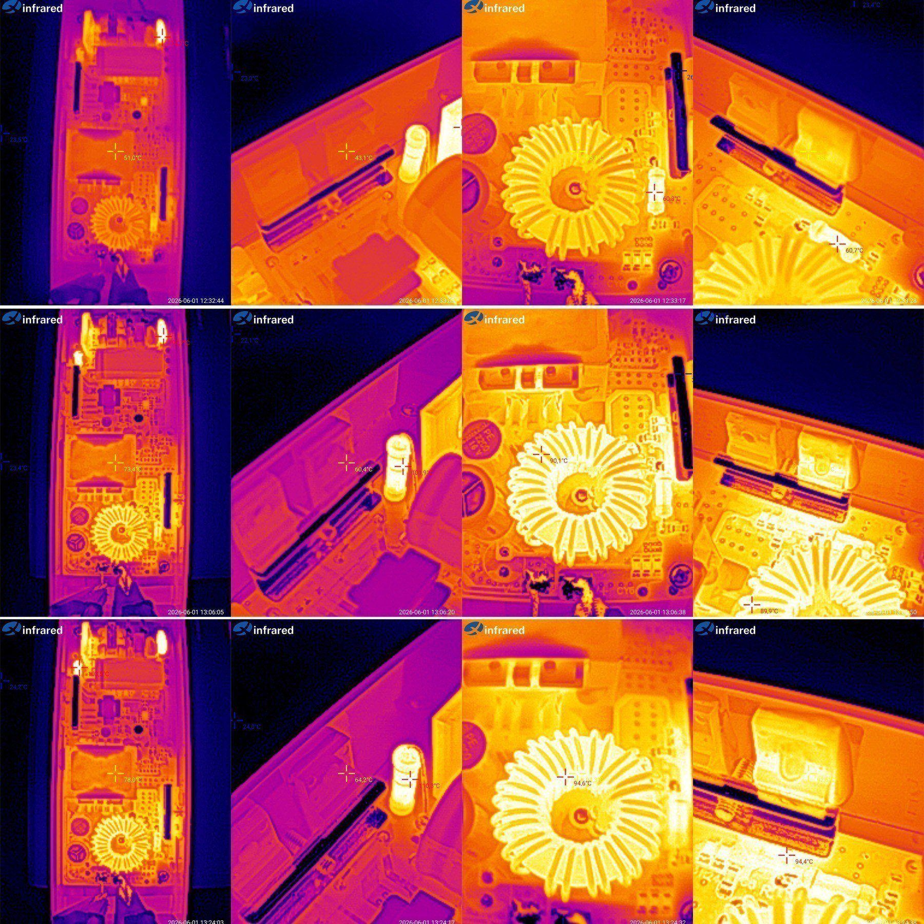
10 A — transformer 51 °C, transistors 43 °C, inductor 55 °C, diodes 56 °C
17 A — transformer 73 °C, transistors 60 °C, inductor 90 °C, diodes 87 °C
18 A — transformer 78 °C, transistors 64 °C, inductor 95 °C, diodes 93 °C.
It’s already clear that even with a 10% overload, at 18 A, the power supply performs very well. The main components have some headroom, and there are certainly no problems at 17 A, even though the rated maximum current for this model is 16.5 A.
I wasn’t too happy with the shunt temperature, though: about 110 °C at an output current of 18 A. So I recommended either adding a second shunt of the same power rating in parallel, or replacing it with a single, higher-power one.
Otherwise, no complaints.
HCF-250-12 power supply, 250 W, 12 V, 21 A — link
This is essentially a more powerful version of the previous model, but I liked it more even at a quick glance. That said, judging anything by appearance alone is pretty pointless.
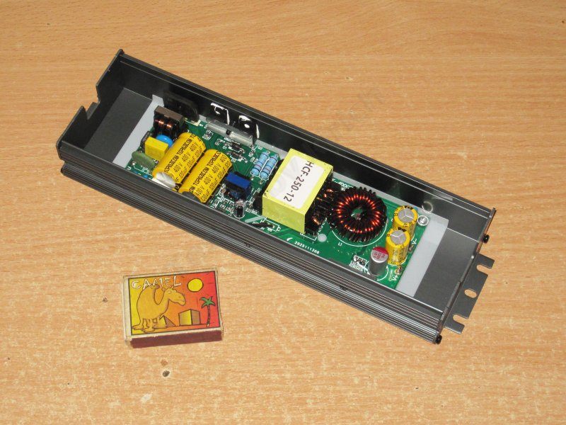
There are now two input capacitors and two shunts, while the output has three capacitors instead of two.
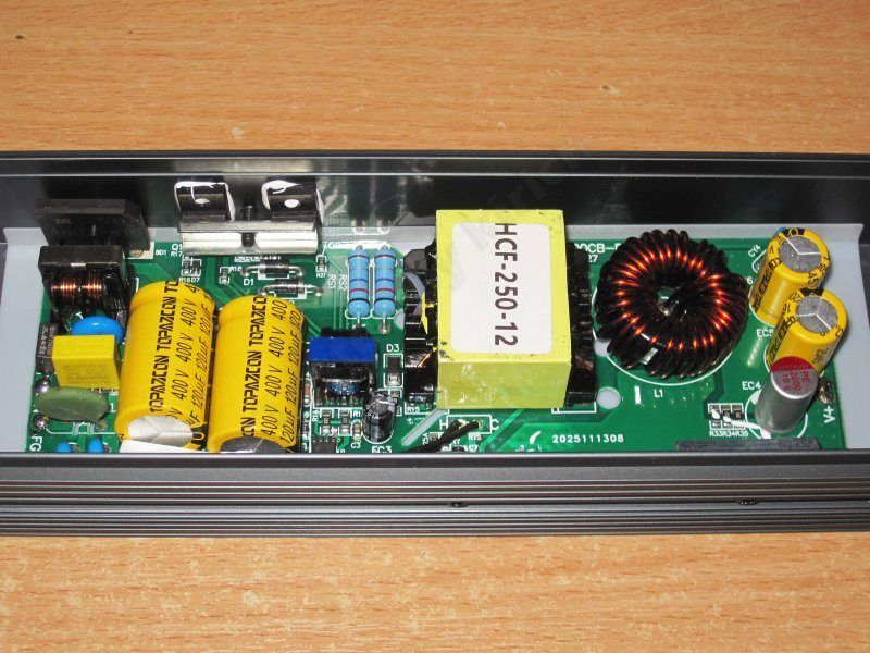
1. Input filter
2. A pair of input capacitors rated at 120 µF; the thermal protection relay is also visible here
3. Transistors mounted with thermal paste; as I mentioned, there are two shunts here.
4. The winding is made from stranded wire, although there aren’t many strands, which is a little odd
5. There are three output diode assemblies. I’ve mentioned before that this topology has “upper” and “lower” diodes, which heat up differently. I think the pair installed here are the ones that run hotter.
6. Output inductor and filter capacitors: one 2200 µF polymer capacitor and a pair of conventional 2200 µF capacitors.
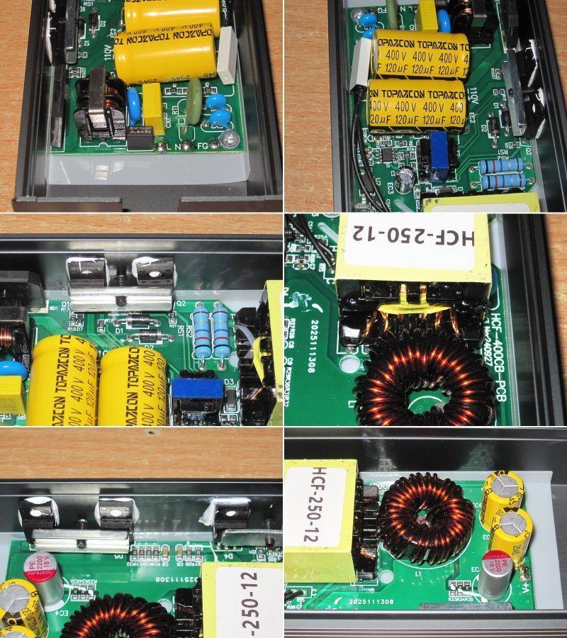
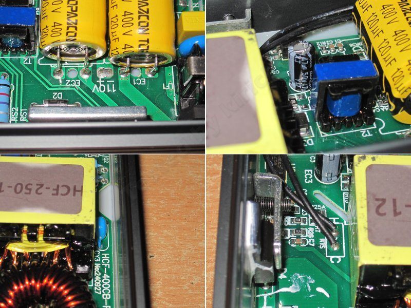
1. Judging by the markings, the capacitors can be configured for 115 V mains, most likely using jumpers.
2. The PWM controller’s supply capacitor is marked Rubycon. We asked them to use high-quality parts, possibly even genuine ones.
3. The Y capacitor is tucked between the transformer and the case.
4. An interesting implementation of overtemperature protection. The thermal protection is connected to the feedback circuit, so when the power supply overheats, it doesn’t shut down completely but reduces the output voltage. I think I’ve shown this before. It’s a very good solution for lighting systems: in the event of a fault, the lights won’t go out completely; they’ll just get noticeably dimmer.
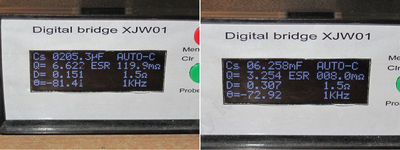
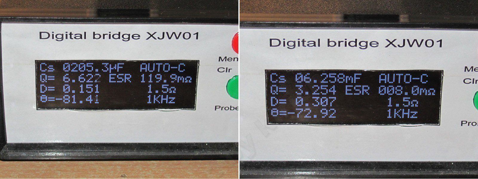
In reality, the input capacitance is about 205 µF, which is perfectly reasonable for 250 W. The output capacitance is about 6250 µF, which is also more than enough for this topology and these specifications.
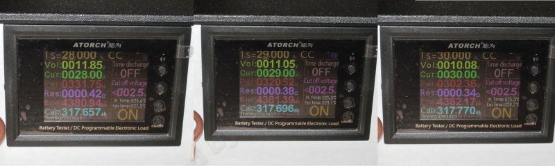
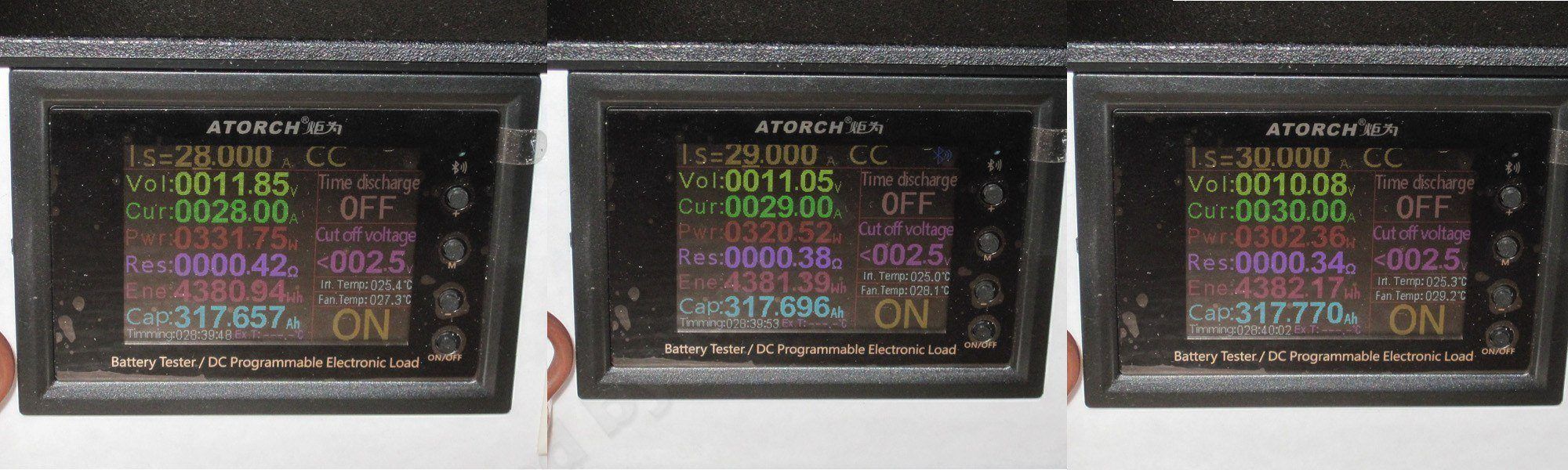
I did have an issue with the protection current being set much too high: the power supply easily delivers 28 A (331 W) despite being rated for 21 A, 250 W. Beyond that, it simply reduces the voltage, but keeps running even with 30 A at the output, delivering 300 W.
I passed this feedback on to the manufacturer, and they started saying something along the lines of: if we lower the protection current, it will shut down much sooner. So, we’ll need to investigate this further, because 28 A is a lot.
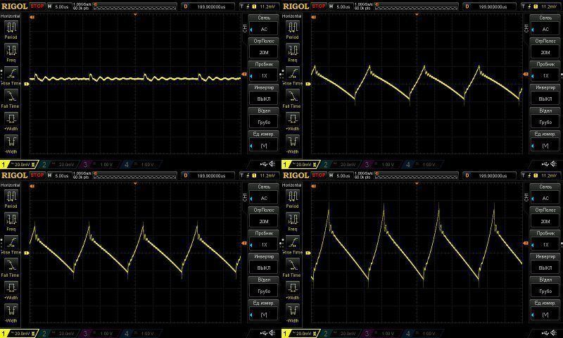
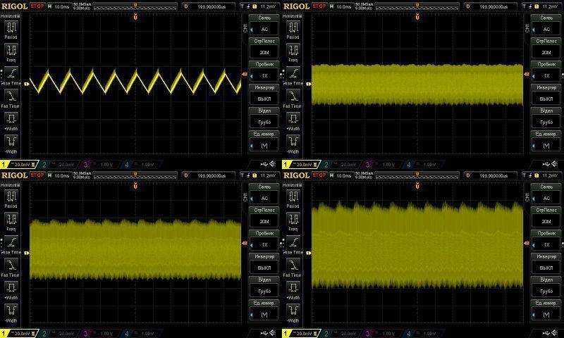
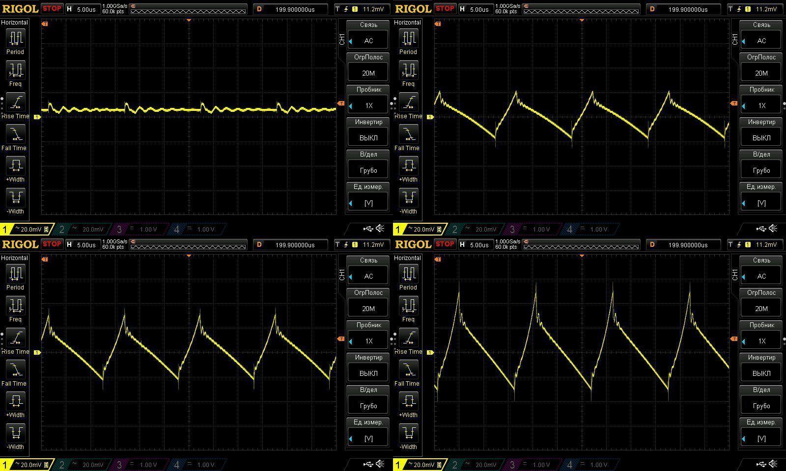
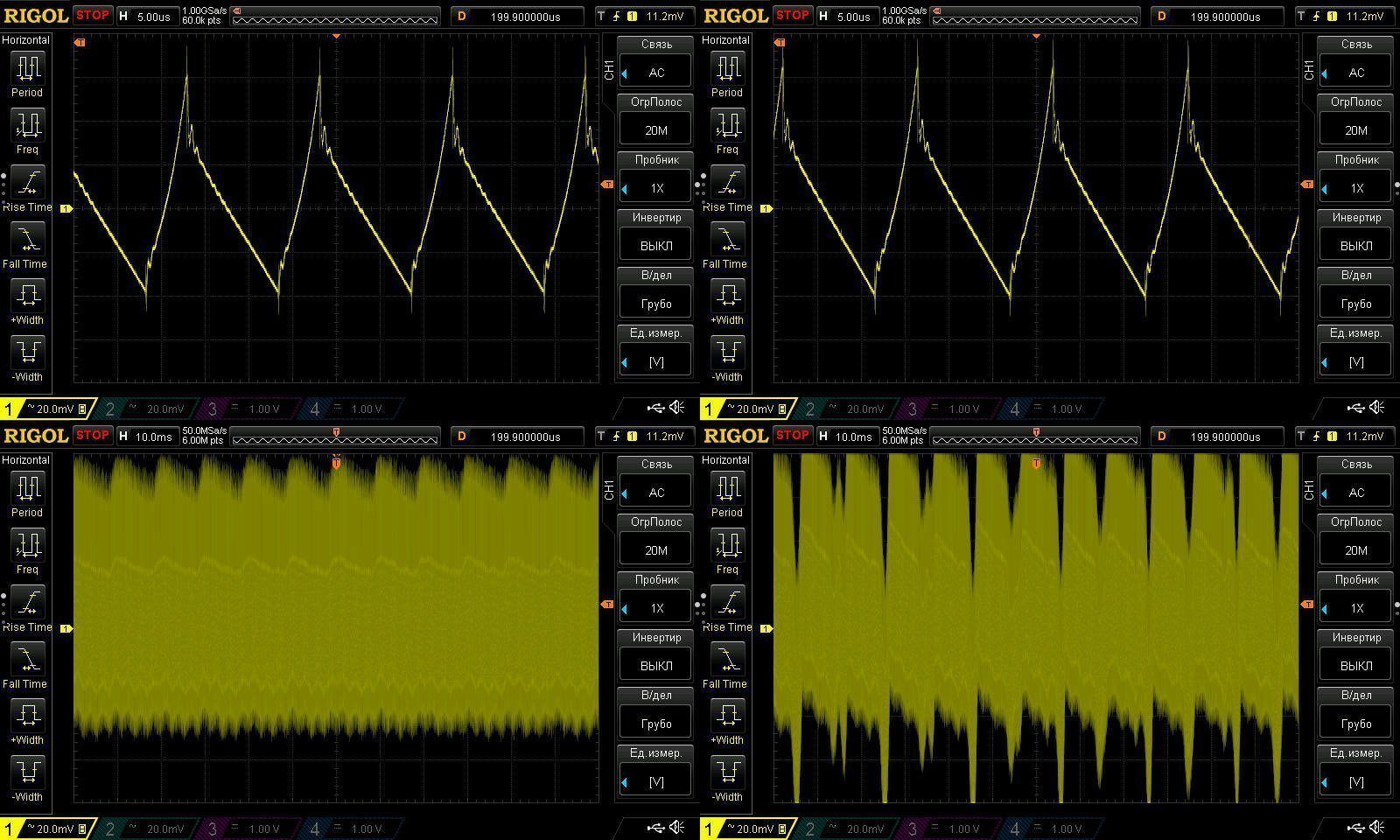
Ripple with no load and at currents of 7, 14, and 21 A.
Here we see the characteristic output waveform of a power supply with this topology. The peak-to-peak ripple is only about 85 mV even at 21 A, which is very good. There are also almost no “spikes,” which is another plus.
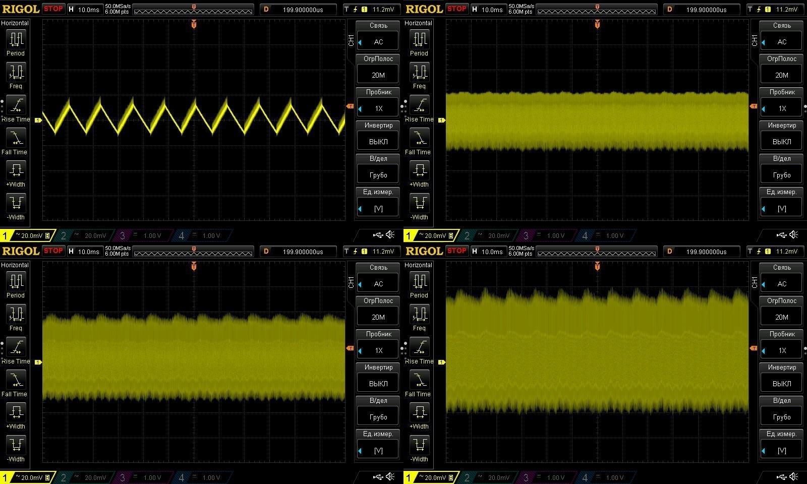
There’s a little 100 Hz ripple visible at the low end, but only a little, and it’s easy to ignore.
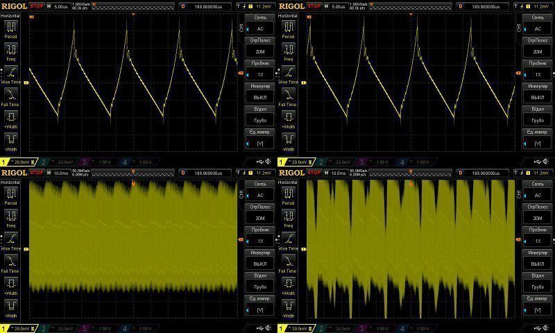
Just out of curiosity, I checked the output at 27 and 28 A.
At 27 A, the ripple has increased, but it’s mostly the low-frequency component that has risen, along with the overall waveform. At 28 A, though, the power supply starts going into protection, and we can see fairly large low-frequency ripple.
On the other hand, even this “large” ripple is only about 200 mV, which is considered normal for quite a few power supplies.
In any case, if your power supply has a gradual rather than stepped protection response, try not to bring the load too close to the trip threshold.
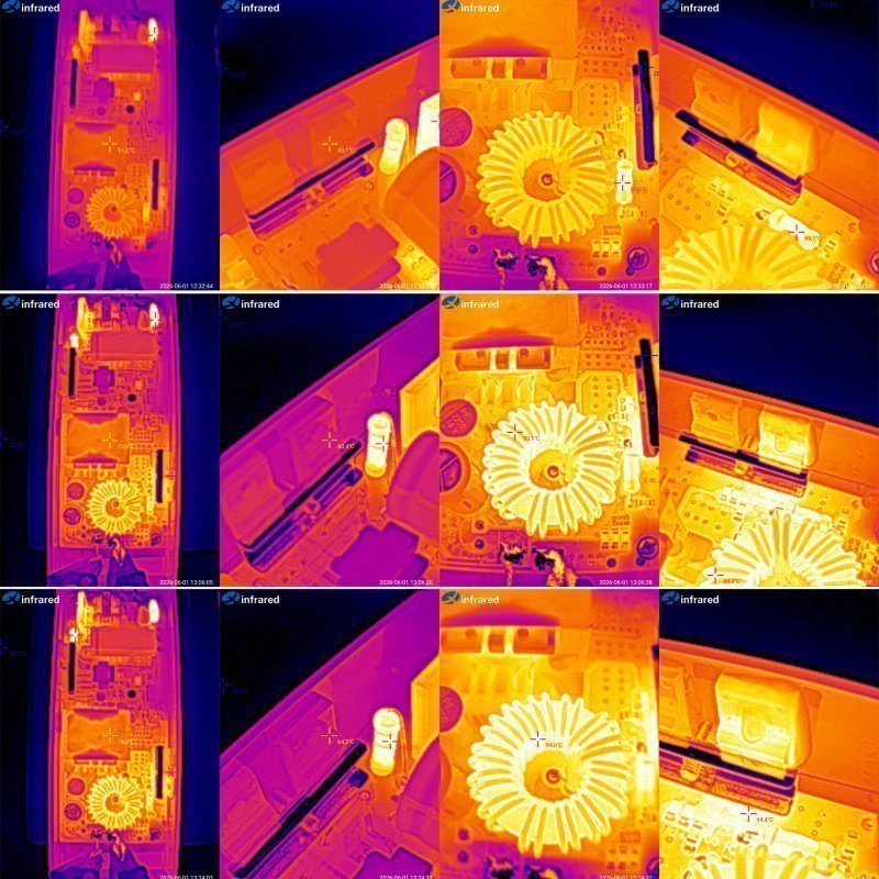
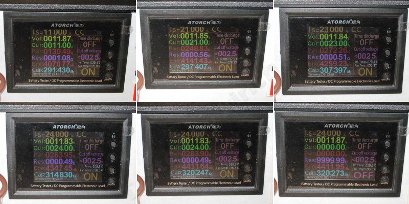
The temperature test was carried out in four stages, at currents of 11, 21, 23, and 24 A. Only the first two are within the rated operating range.
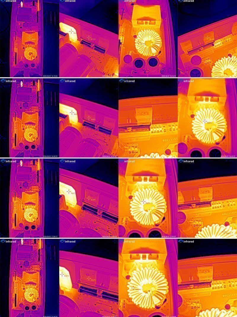
Here are the temperatures of the main components:
11 A — transformer 55 degrees, transistors 37, inductor 61, diodes 46
21 A — transformer 77 degrees, transistors 55, inductor 90, diodes 73 (sorry, I mixed up the last two photos in the series)
23 A — transformer 83 degrees, transistors 61, inductor 98, diodes 78 degrees.
24 A — transformer 88 degrees, transistors 65, inductor 103, diodes 82 degrees.
In my opinion, this power supply performs very well not only within its rated operating range, but also with almost a 15% overload—and that’s without potting it in compound.
Even under overload, there’s a little headroom. The inductor is under the most stress, while the other components are operating in “greenhouse” conditions.
And now, the two most powerful power supplies in the lineup, the HCF-320-12 and HCF-320-24 — link
The models shown are almost identical; the key difference is the output voltage, 12 or 24 V. I’ll start with the 12 V model.
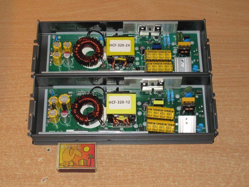
1. A full input filter, a heatsink on the bridge rectifier, and a pair of 150 µF capacitors in parallel at the input.
2. The transistors are clamped down through a heat-spreading plate. I’m not sure there’s thermal paste under the plate, though; the tests will show how it all works.
3. The transformer’s secondary winding is made with fairly thick Litz wire.
4. A thermal protection switch is clamped between the output inductor and the transformer.
5. There are four output diode assemblies, clamped down through a large heat-spreading plate.
6. An interesting combination on the output: one 2200 µF polymer capacitor and three conventional ones—two 2200 µF and one 3300 µF.
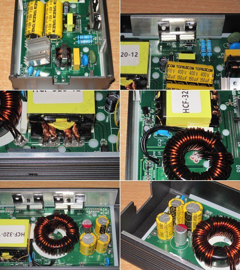
The thermal switch is rated for 80 degrees. The protection works the same way: it reduces the output voltage.
A couple of 2 kΩ ballast resistors are tucked away near the capacitors :)
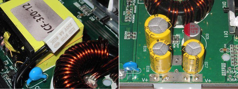
For testing all power supplies rated at 150 W and above, I used a 1200 W load based on Atorch, with a four-wire connection. A reminder: I make electronic loads rated from 1200 to 5400 W, with currents from 50 to 240 A.
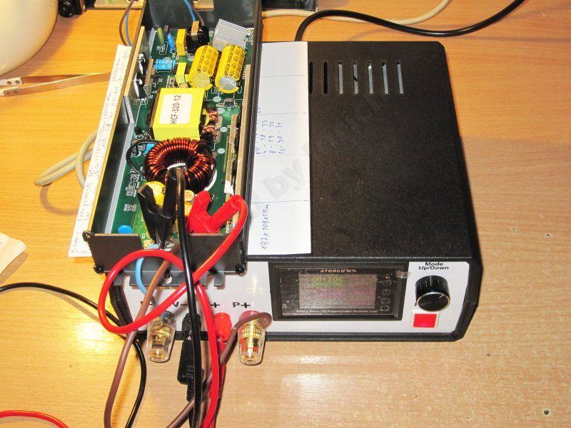
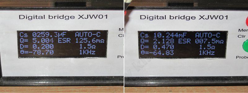
The input filter capacitance is 260 µF, which is fine. As I mentioned, this power supply operates over a “narrow” range, usually 198–260 V.
The output capacitance is 10200 µF, which is more than enough for the specified ratings.
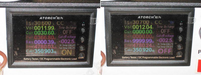
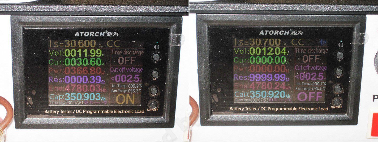
The protection has a fixed threshold and trips at a current of about 30.7 A.
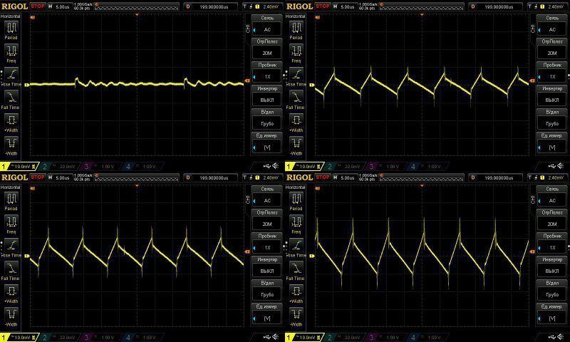
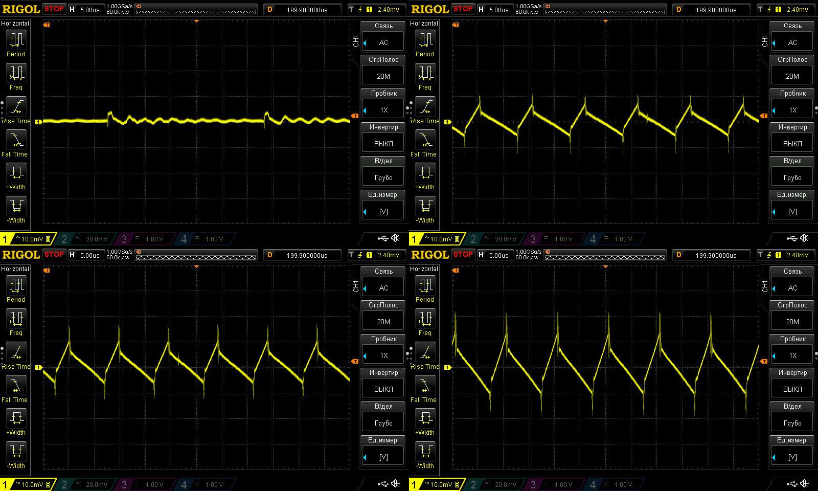
Ripple with no load and at currents of 9, 18, and 28 A.
This is genuinely impressive: even at 28 A (336 W), the peak-to-peak ripple is only up to 40 mV. That’s great.
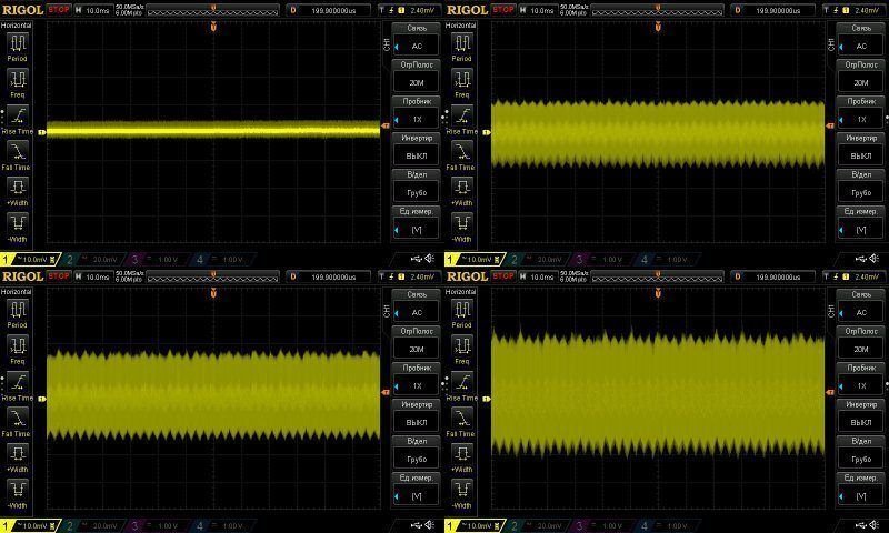
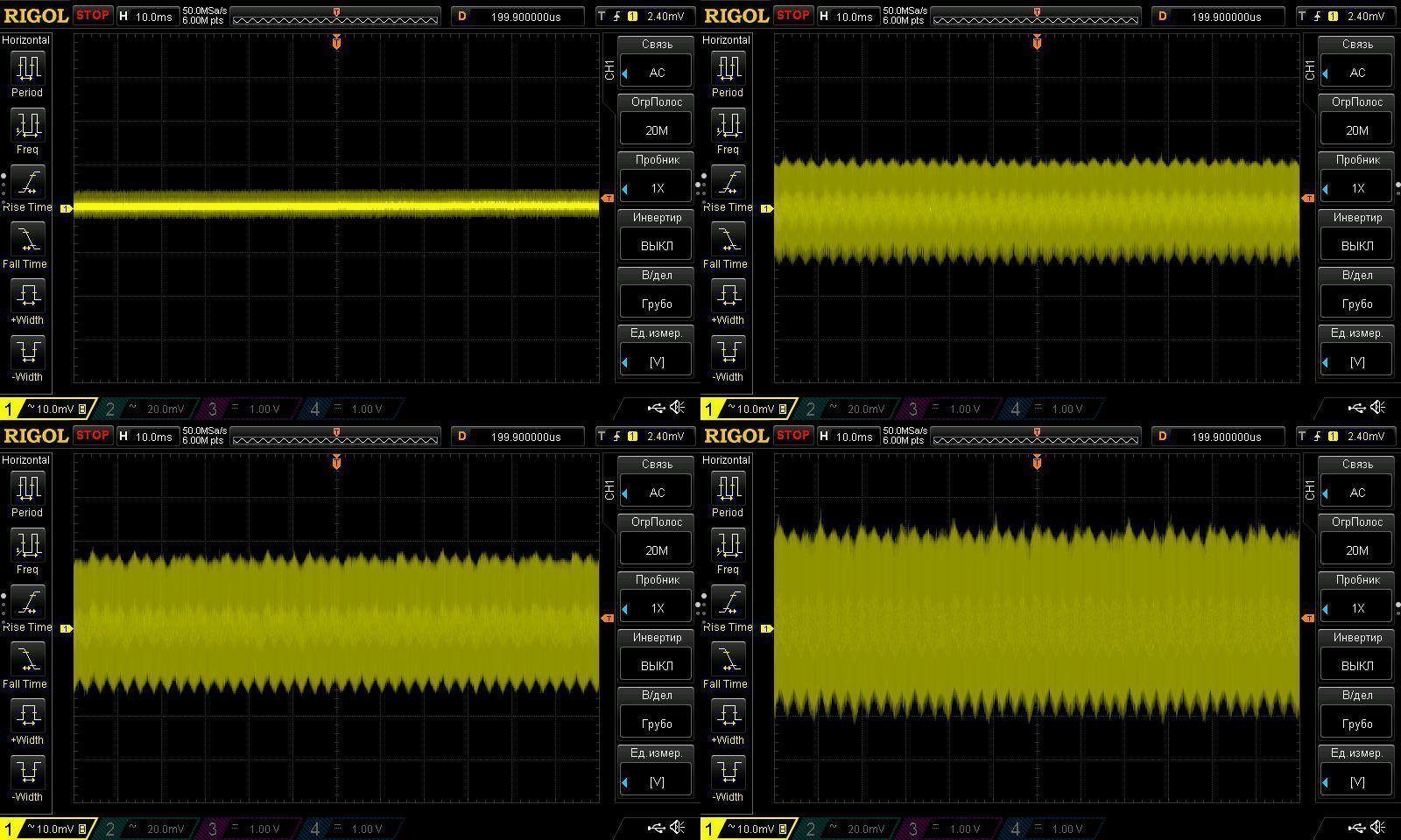
The low-frequency waveform is just as good—really nice to look at.
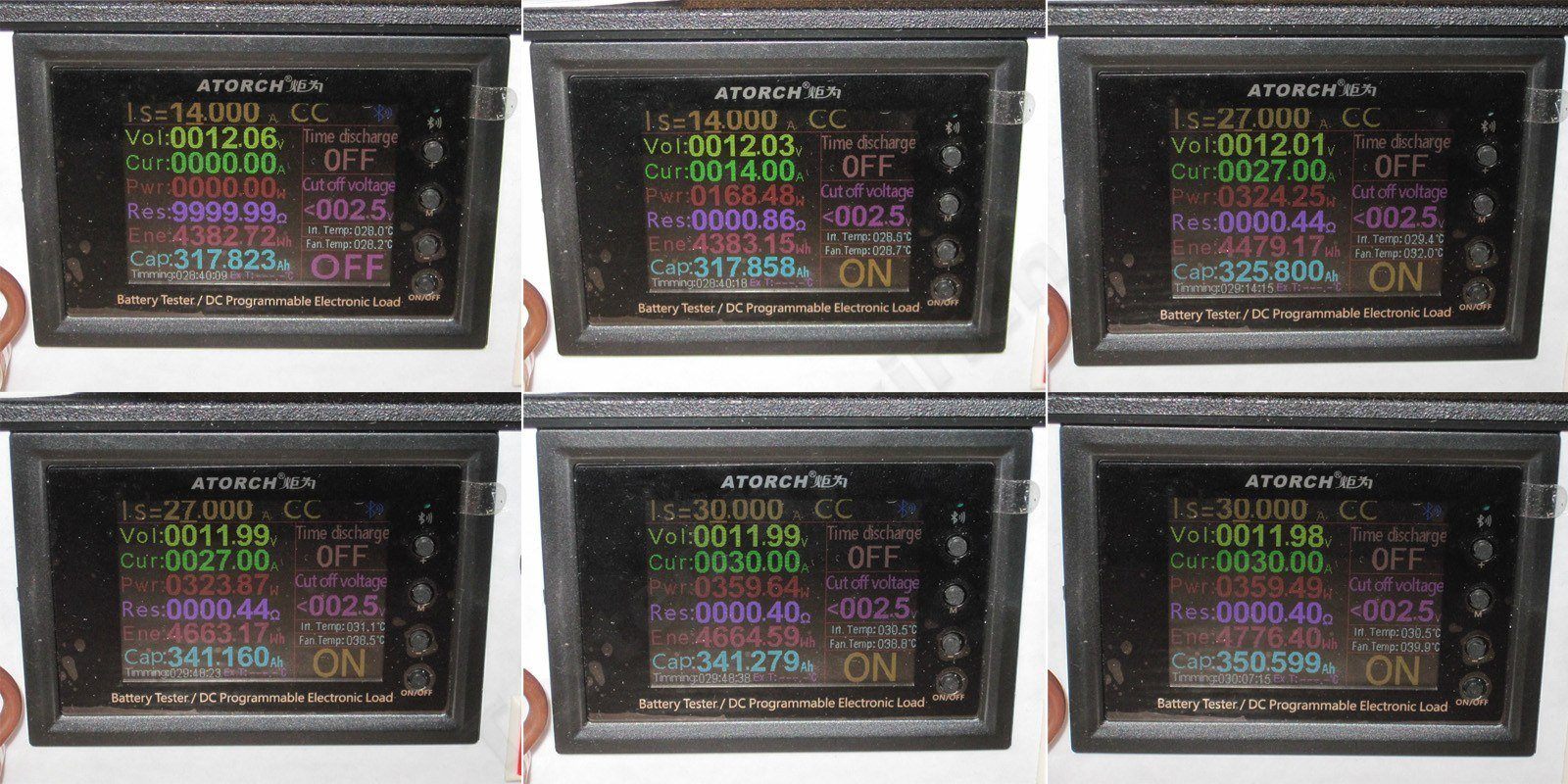
The power supply was tested at load currents of 14, 27, and 30 A. Yes, I decided to put it through its paces at 360 W as well.
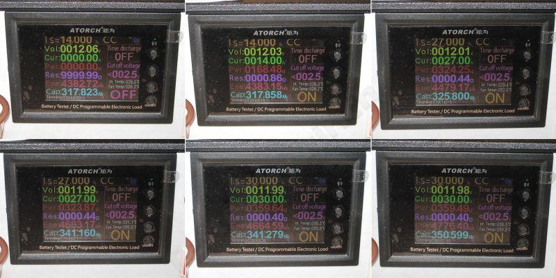
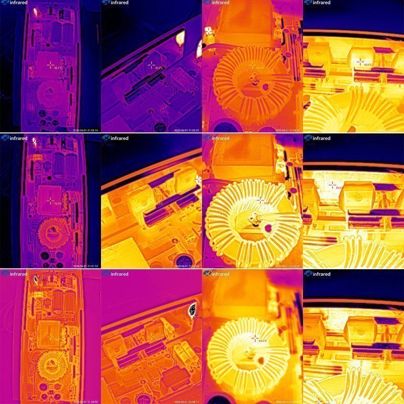
And now for the component temperatures.
At 14 A: transformer 45 degrees, transistors 42 degrees, inductor 46, and diodes 48.
At 27 A: transformer 70 degrees, transistors 70, inductor 84, and diodes 81 degrees.
At 30 A: transformer 79 degrees, transistors 80 degrees, inductor 95, and diode assemblies 88 degrees.
I think it's obvious that there's even a noticeable margin for operating at 360 W, let alone at 27 A. And that's without potting it with compound, which I think would lower the inductor temperature a little.
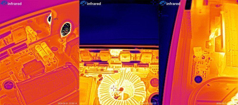
At maximum current, the shunts reach about 100 degrees, which is normal.
As for the diode temperatures, they don't heat up evenly; I measured the maximum temperature at each point.
I noticed some heating of the TL431 zener diode, which is a little puzzling, but the temperature isn't very high—about 77 degrees. It's just higher than I'm used to seeing.
And the 24 V version, HCF-320-24, with a voltage of 24 V and a current of about 14 A — link.
For the most part, I'll be comparing the 12 V and 24 V versions from here on.
The input sections are identical, apart from differences in the PCB layout.
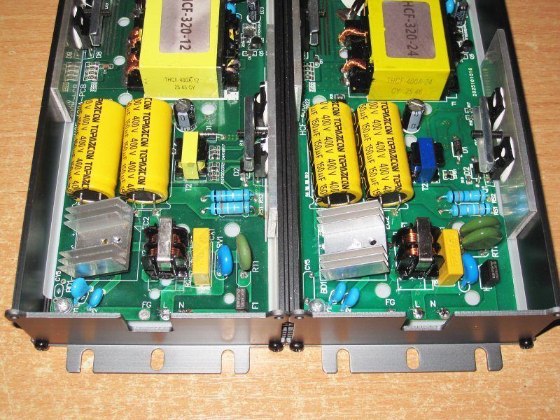
Look closely and you'll see that the boards are different, but the difference is between revisions and has nothing to do with the power supply voltage. The 24 V board is simply newer.
When we pointed out some shortcomings—which, by the way, were more numerous in the 12 V version—we were told that the board was being revised, so the 24 V version is better. As I understand it, they gradually collect suggestions for improvements and then implement them all at once, so there may be another version later that incorporates my suggestions.
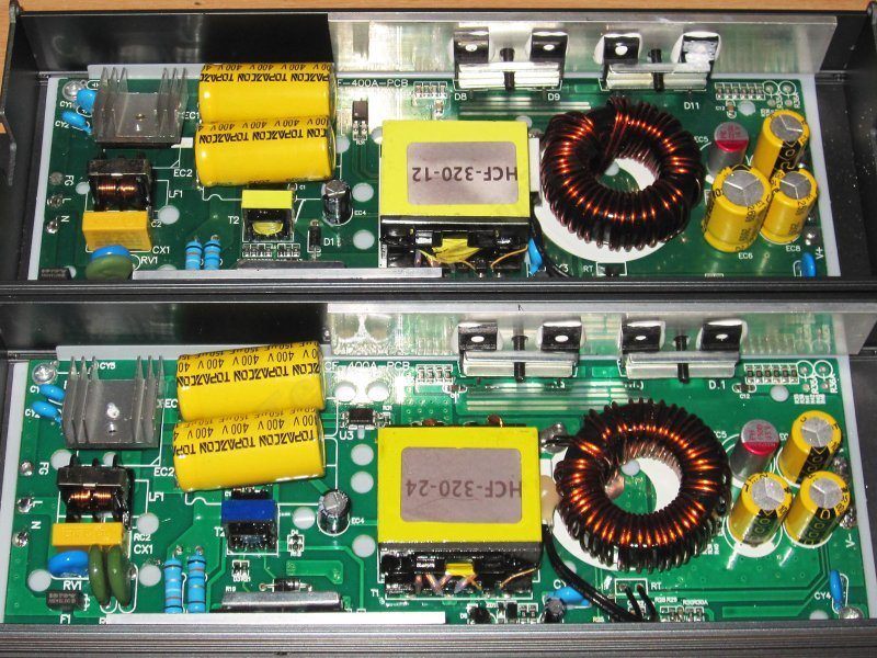
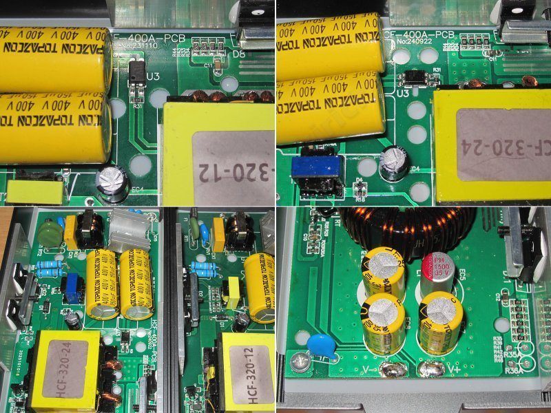
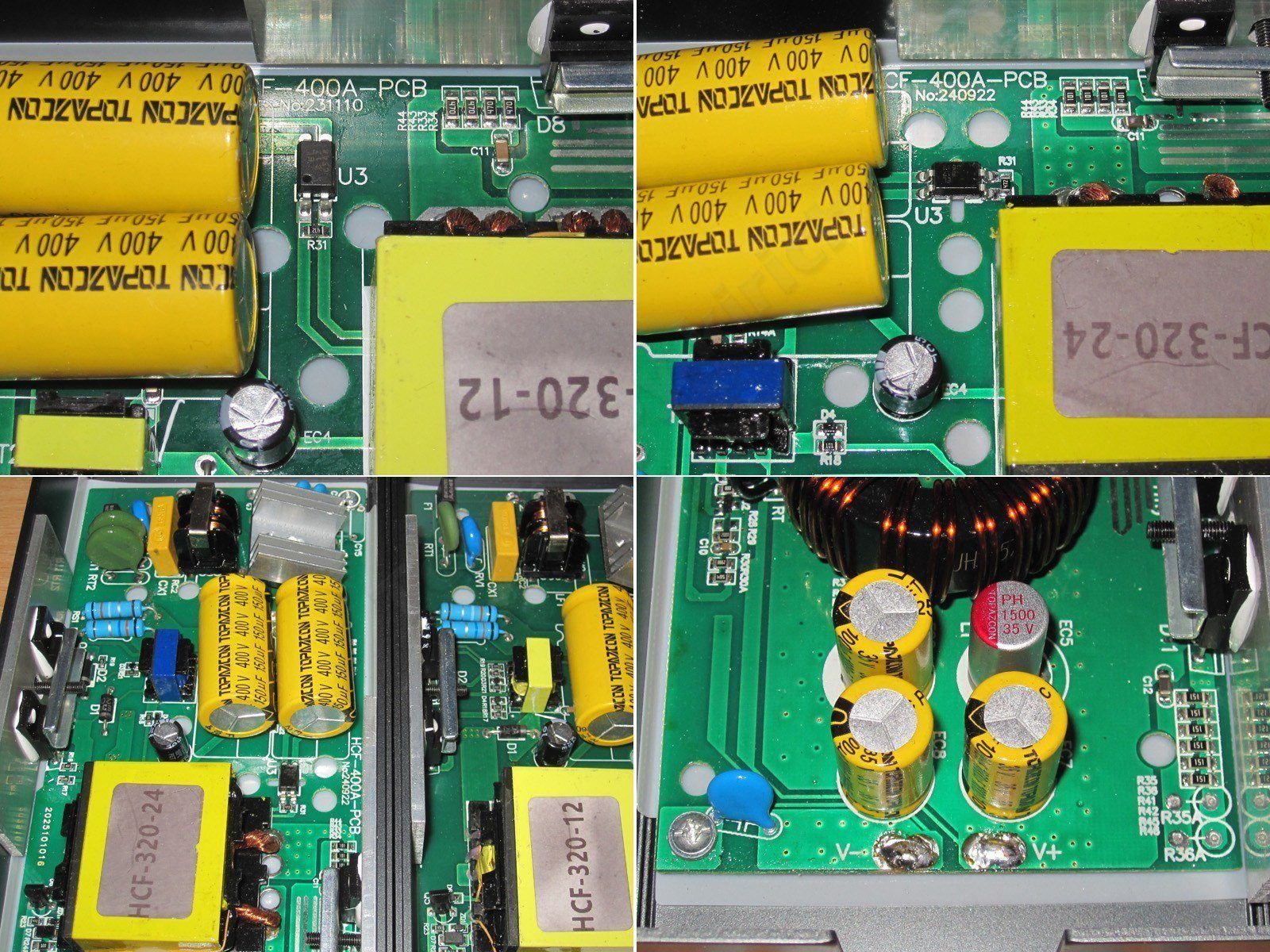
1, 2. The difference between the board versions is visible at the top. You can also see that the optocoupler has already been moved; I haven't thought about why.
3. You can also see that the 24 V board (on the left) looks emptier around the high-voltage section. Perhaps some components have been moved to the underside.
4. On the output, there are 35 V capacitors: one 1500 µF polymer capacitor and three regular 1000 µF capacitors. And yes, the layout of the power planes here is also quite different from the 12 V version.
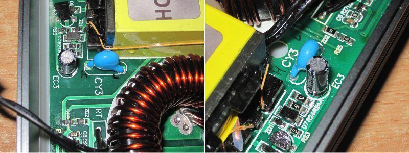
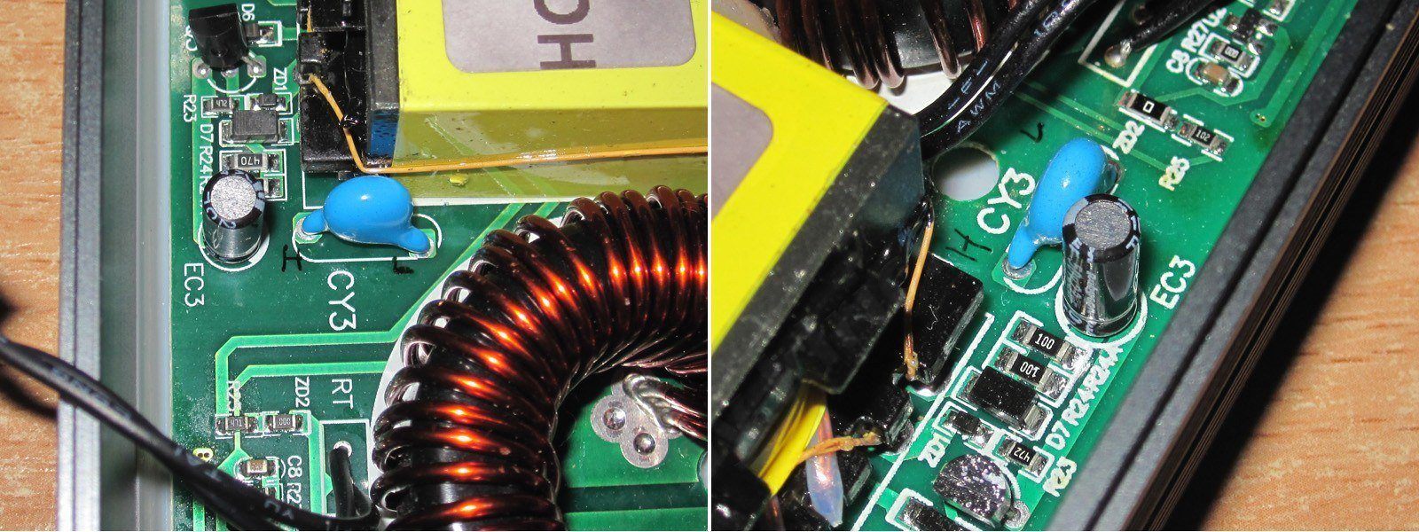
My concern was the placement of the Y capacitor. Its leads are marked H (hot side) and L (cold side).
You can see that the H lead is quite close to the feedback circuit. With potting compound, this isn't as critical as it would be in an open design, but personally, I don't like either option.
I brought this up with the manufacturer and sent them a photo.
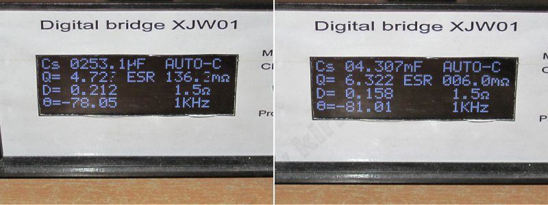
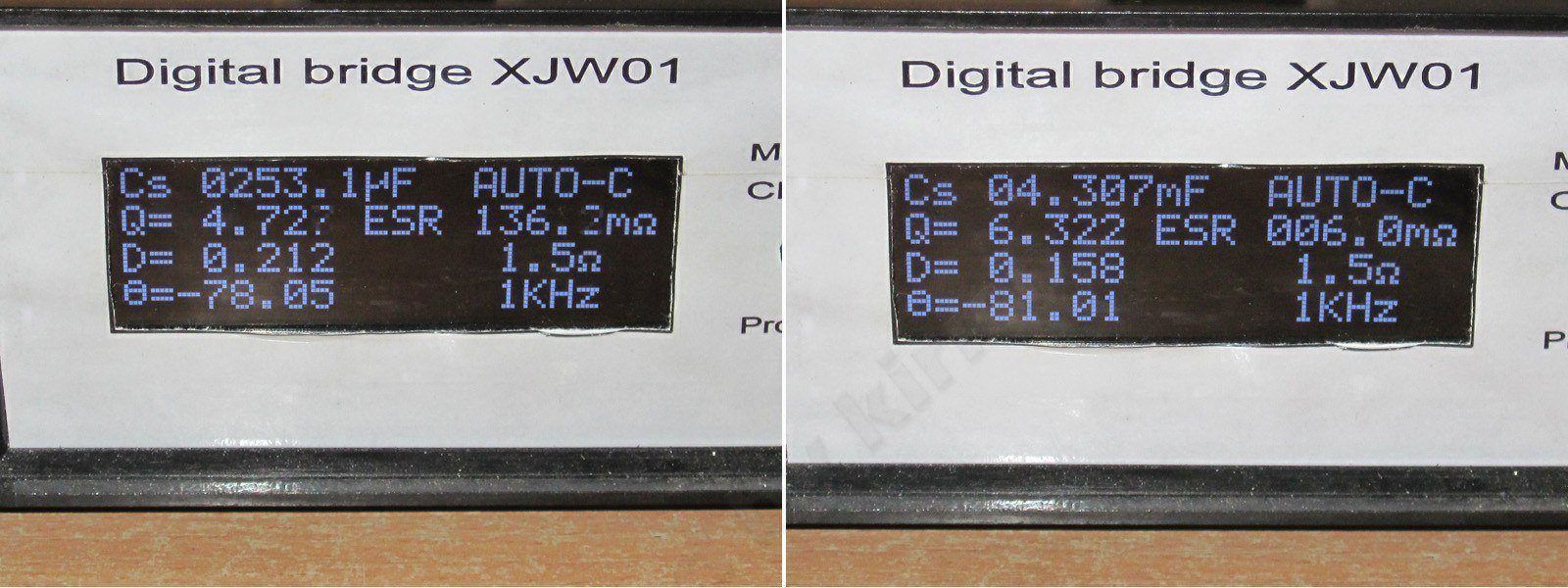
The input filter capacitance is 253 µF. For comparison, the Mean Well LRS-350 has a 280 µF input filter, so they're comparable.
The output capacitance is 4300 µF, which is more than adequate for this topology and a current of around 14–15 A.
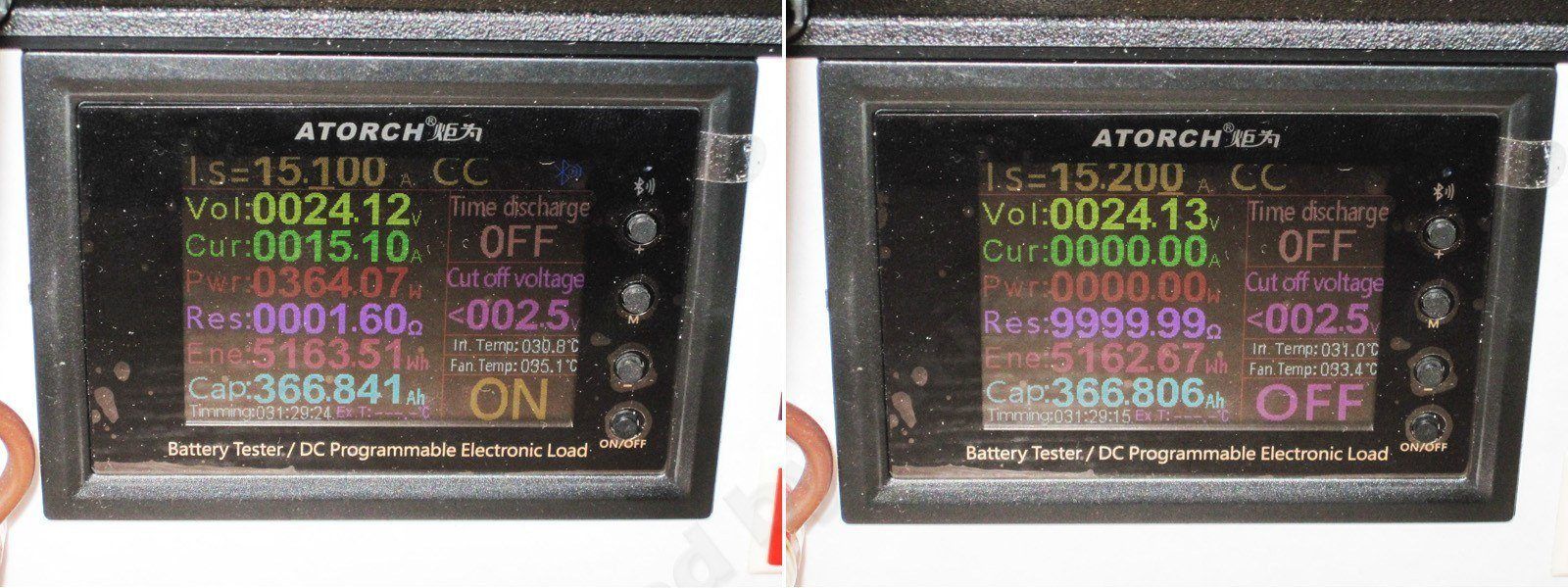
The protection is also threshold-based and set to about 15.2 A, which is half the setting of the 12 V version, as you'd expect.
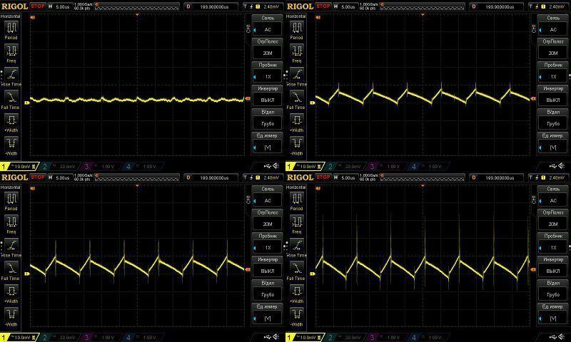
I captured the waveforms with no load and at currents of 5, 10, and 13 A.
Overall, they look good, except for the “spikes,” which I've never liked :)
But in practice, even taking everything into account, the total ripple is about 40 mV, which is negligible given the output voltage. An excellent result.
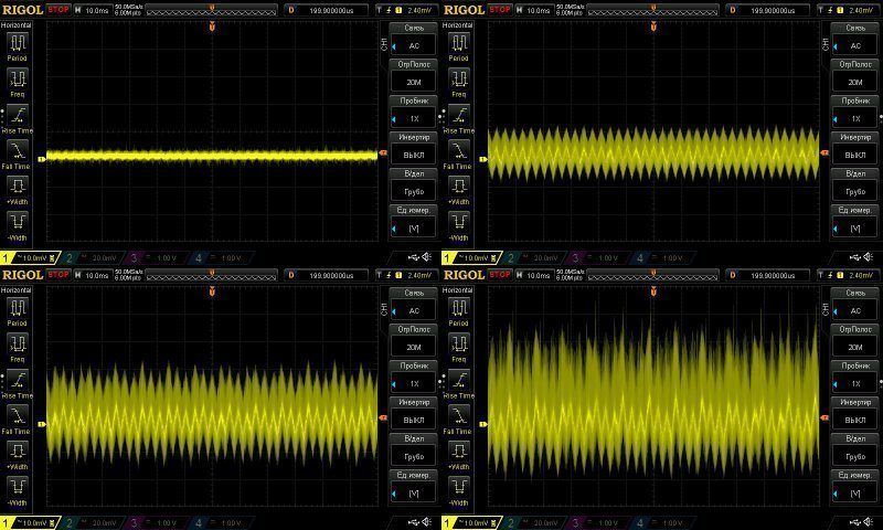
At low frequency, the waveform looks more like “wool,” though it's still excellent here. One division on the screenshot is 10 mV, so this is an excellent result.
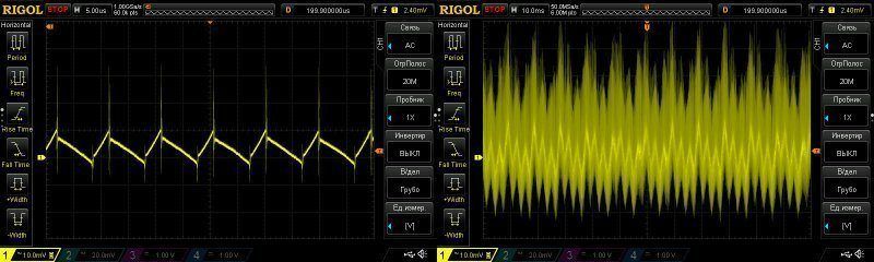
Even when the power supply is loaded right up to its limit at 15 A, the picture doesn't change much. The ripple increases a little, but that's about it.
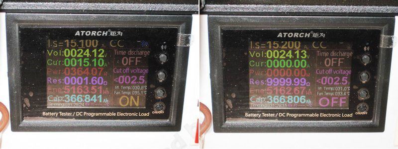
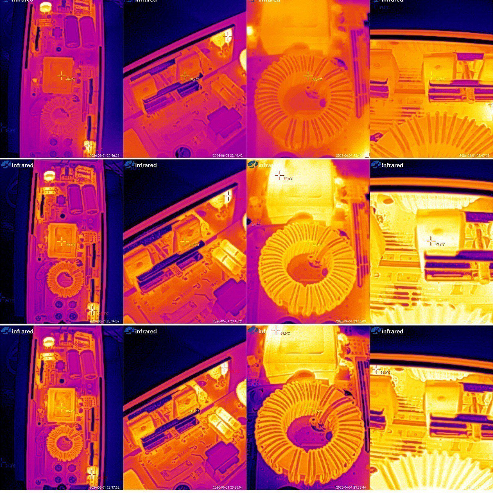
I checked the temperatures under load in three modes: 7, 14, and 15 A, again at maximum load. That is, The final test at maximum power.
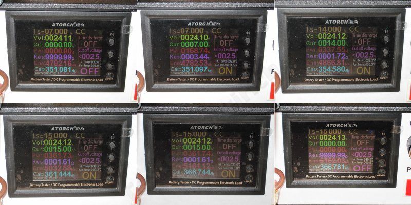
Now for the interesting part: temperatures.
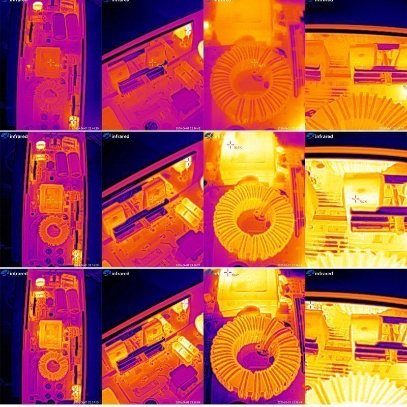
7 A — transformer 50 degrees, transistors 50 degrees, inductor 46 degrees, and diodes 49 degrees
14 A — transformer 79 degrees, transistors 81 degrees, inductor 74 degrees, diodes 73 degrees.
15 A — transformer 86 degrees, transistors 88 degrees, inductor 81 degrees, and diodes 77 degrees.
Interestingly, temperatures here are higher for everything except the inductor than on the 12 V version. The inductor runs cooler, though, so the power supply is better balanced and, even as it is, has roughly 15–20 degrees of headroom.
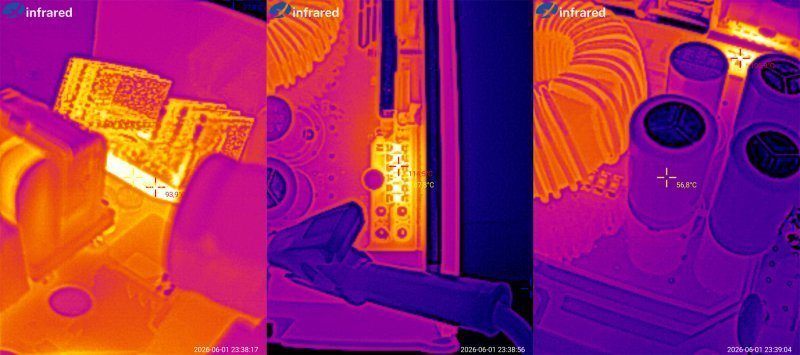
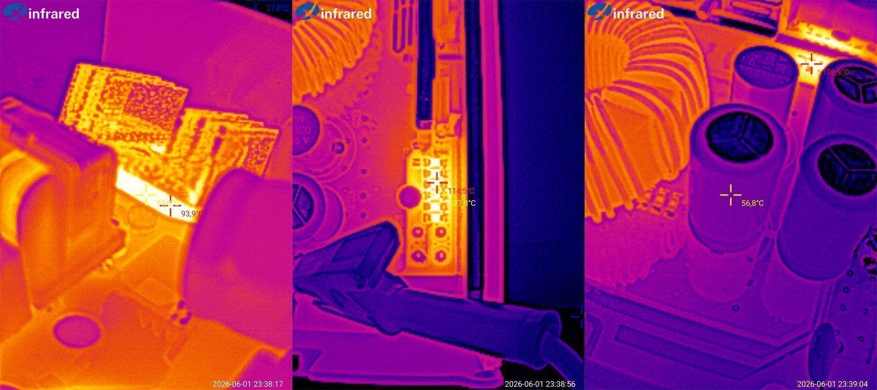
The bridge rectifier reached 94 degrees, which is also fine. The output snubber got noticeably hot at 114 degrees; I think potting it with compound should help. The capacitors reached 56 degrees, and here the effect will be the opposite: their temperature will rise after potting.
Proper placement of the power components makes quite a difference. The transistors transfer heat to one side of the case, and the diodes to the other, so the case works more effectively as a heatsink than if they were all on the same side.
Conclusions.
HCF-36-12: a small, simple power supply. The main issue is that the varistor is connected before the fuse; that’s not how it should be done.
HCF-60-12: simply a decent power supply, with hardly anything to complain about.
HCF-100-12: the transformer got noticeably hot at 8.4 A and very hot at 10 A, but I think potting it with compound should bring the temperature down.
HCF-150-12: no complaints.
HCF-200-12: a few minor issues with ripple and inductor temperature, but overall everything is within normal limits.
HCF-250--12: no complaints, although the output inductor gets noticeably hot at currents above the rated maximum. At 21 A, everything is fine. The power supply can handle 280 W without a problem, in principle.
HCF-320--12 and HCF-320-24: two great power supplies. I’d say there’s nothing to complain about, but there are a few things. On the 12 V version, the inductor got noticeably hot at 30 A (360 W); I think potting should fix that. There are also some issues with the Y capacitors, or rather, their placement.
One thing almost all these power supplies have in common is low ripple. The exception is the 36 W model, which has no output filter.
I also hope replacing the capacitors will improve reliability, since it has already had a positive effect on ripple.
Overall, all the power supplies performed quite well, especially considering that I tested them not only at their maximum rated operating conditions, but also under significant overload. Even then, I had very few complaints.
That’s all for today. As always, thanks to Vitaly for providing the samples for testing.
As a reminder, to keep up with new posts on the blog, I recommend following me on Instagram. I'll post notifications about all new posts there, and might also write about something interesting from time to time: link to account
You can also subscribe to updates and new articles on the Telegram channel - https://t.me/KirichBlog Note that discussions of reviews and articles are enabled on the channel, as is general chat. I recommend it.
As I've written before, we're trying to get power supplies that offer the best balance of quality and price. So we take some basic models, test them, send our recommendations to the factory, and they incorporate the changes into the production units.
Today's article is a case in point.
The goal is simple: with a minimal increase in the product's price, we want to get:
1. Better safety, through certain components and circuit board layout.
2. Better reliability, meaning a longer service life and operation over a wider temperature range.
3. Better power quality. For example, what's the point of a power supply with high efficiency and excellent reliability if it dumps ripple into the load?
That's exactly why we make these optimizations. But people sometimes mean different things by “optimization.”
One kind of optimization is to cut the price by removing the input and output filters and using components that are pushed to their limits. Sure, the price goes down, but quality takes a serious hit.
Another kind of optimization, for example, is replacing a component mounted on a heatsink with a more efficient one. Interestingly, this often has almost no effect on the price: even if the new component costs more, you may no longer need a heatsink, and the component being replaced wasn't free either. The usual bonus is higher efficiency, which means less heat and better reliability.
We stick to the second kind of optimization, but unfortunately, we often see the first kind in our market—and elsewhere.
So, today's article will cover 8 power supplies rated at 36, 60, 100, 150, 200, 250, and two at 320 W.
As you can see in the photo, there are clearly more power supplies than that. After testing, we simply didn't like the 50 W model, so it was replaced with a 60 W version. As for the 40 W model, you'll see why as you read on.
Someone will of course say, “What's the point if the Chinese can just do whatever they want, especially since the unit is sealed?”
No. From time to time, we can randomly select a unit from a batch, take it apart, and compare it with the sample—especially since we have detailed photos. If they substitute anything, we file a complaint with the factory. We need consistency.
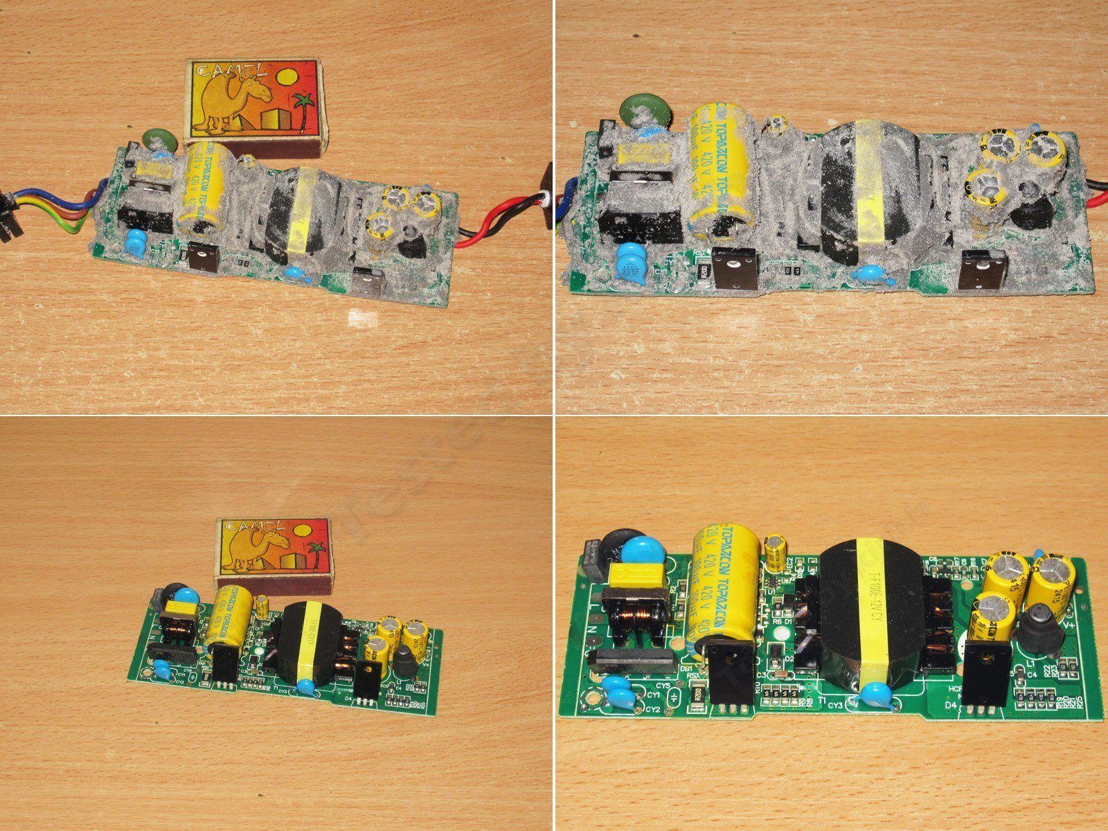
And of course, I'll start with the 36 W model, i.e. 12 V, 3 A. - link
I'll show this model alongside the 40 W version, but I didn't even test the 40 W one because I didn't think it was worth doing.
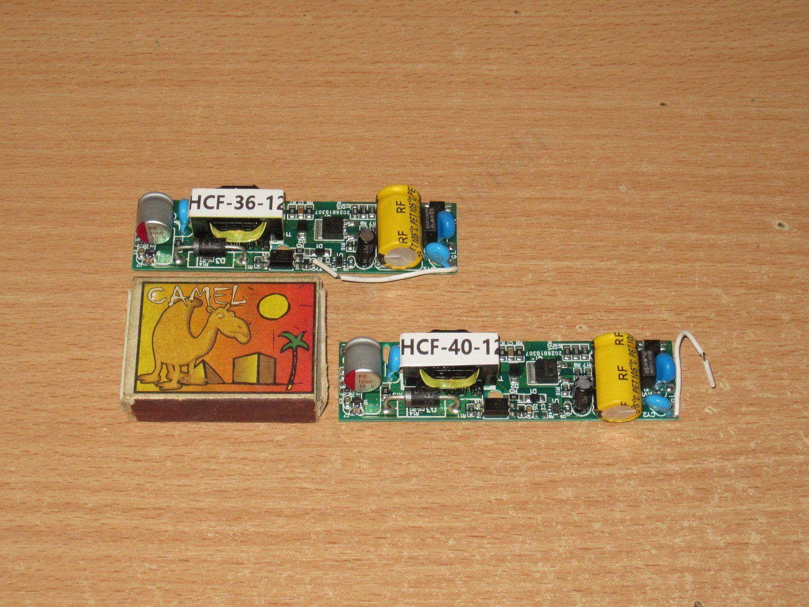
I think this photo makes it clear why I tested only the 36 W model: the boards are identical. What's interesting is that the Chinese set different prices for them, which is reflected in the store price.
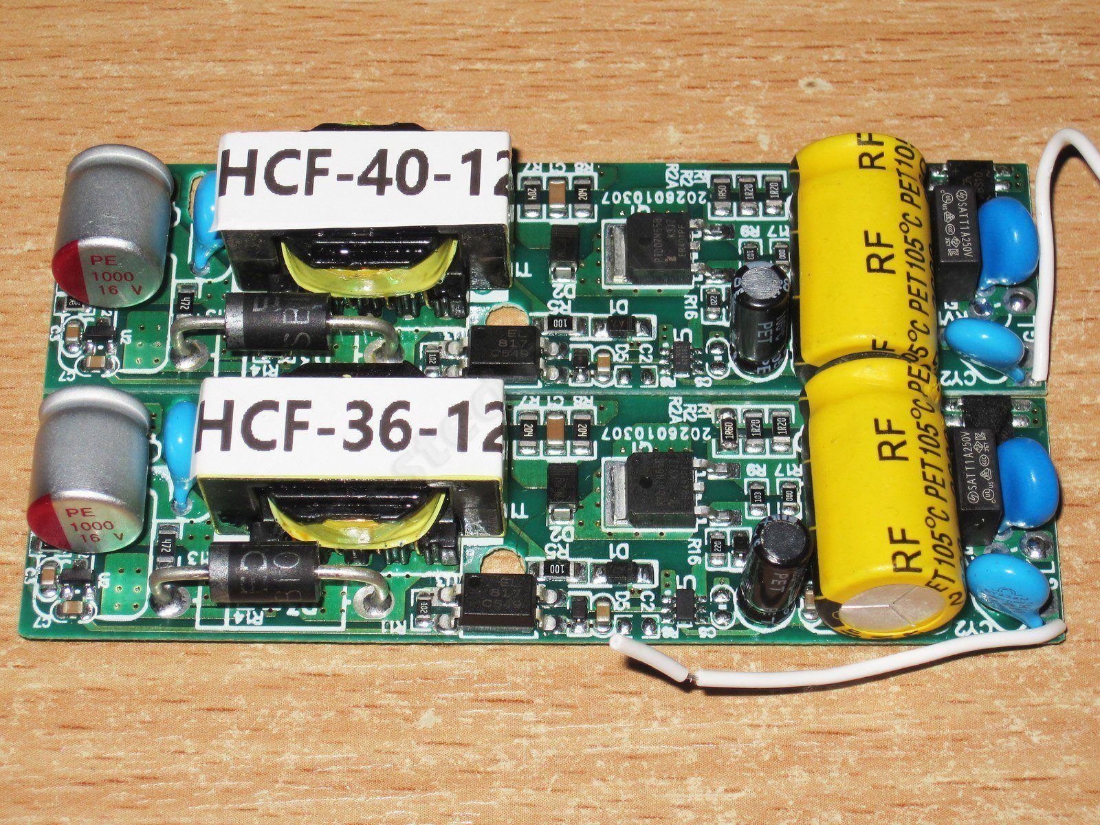
1. There's no input filter. This is the most basic model in the series, but it does have a varistor.
2. The input capacitor is 33 µF.
3. The key difference between the units is the value of one of the shunt resistors.
4. At our request, the manufacturer installed more reliable capacitors, marked Rubycon, though I can't vouch for them.
5. There's a proper capacitor between the primary and secondary sides.
6. At our request, the standard output capacitors were replaced with polymer ones.
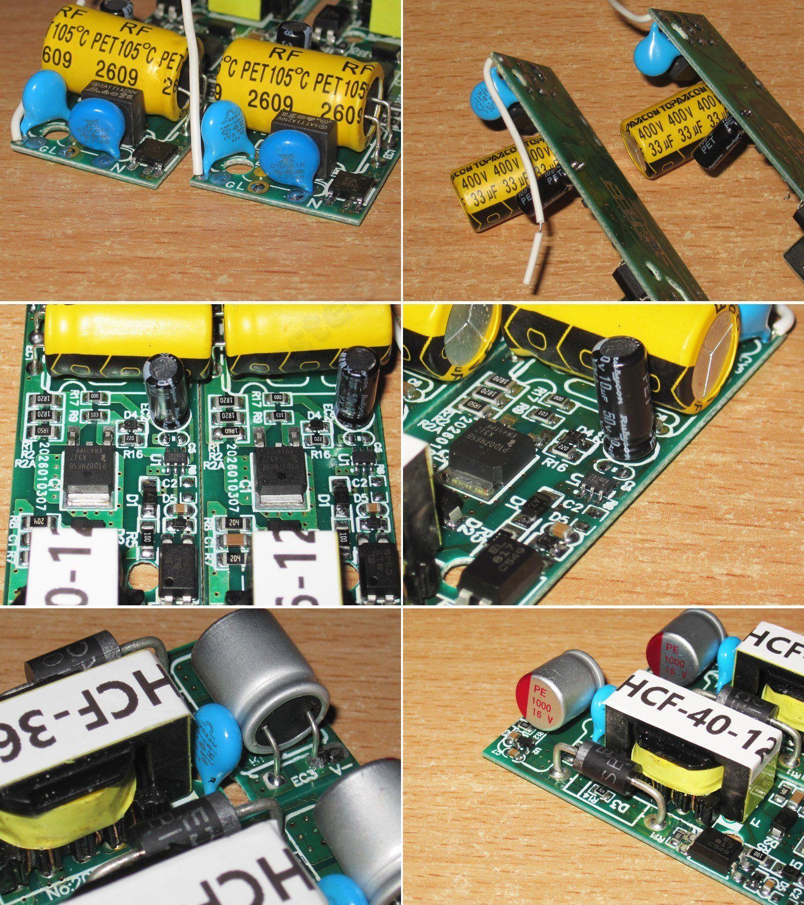
No issues with electrical safety.
But the varistor issue definitely needs fixing: you mustn't connect a varistor across the input before the fuse.
The actual input capacitance is about 28 µF. That's fine for a 230 V mains supply, but too low for 115 V. With a low input voltage, you should either not load it to 100% or expect problems.
The output capacitance is 880 µF. Since these are polymer capacitors, that's definitely better than before.
The protection current is set to 3.1 A; beyond that, the power supply starts reducing the voltage. Everything looks fine here. The protection current does not depend on temperature.
Ripple with no load and at currents of 1, 2, and 3 A.
I have no complaints about the main part of the waveform, but the “spikes” are a bit too large. Several things could be causing them: the snubber, the PCB layout, or even the fact that the output capacitor is lying flat rather than being soldered upright. The last explanation is quite plausible.
At low frequencies, the main component is actually caused by the “spikes,” which makes the waveform look rather poor.
I ran the thermal test at 50% and 100% power for about half an hour each. The output voltage is practically unaffected by temperature.
At 1.5 A, the transformer reached 69 degrees, the transistor 62, and the output diode 85.
At 3 A, the transformer reached 104 degrees, the transistor 90, and the output diode 133.
That’s quite a lot, but bear in mind that the power supply isn’t potted in compound, which also helps distribute heat. Incidentally, the 40 W power supply will run at an even higher temperature.
Also bear in mind that I’m testing it at 100% power, although continuous operation at full power is generally not recommended.
60 W power supply, 12 V, 5 A - link
This is where the difference starts to show between the power supplies I tested earlier and the one I’m showing today.
The thing is, the boards I received back then were bare, and I used my own heatsinks. This one has the original heatsinks, so we can see how the cooling is implemented under the potting compound.
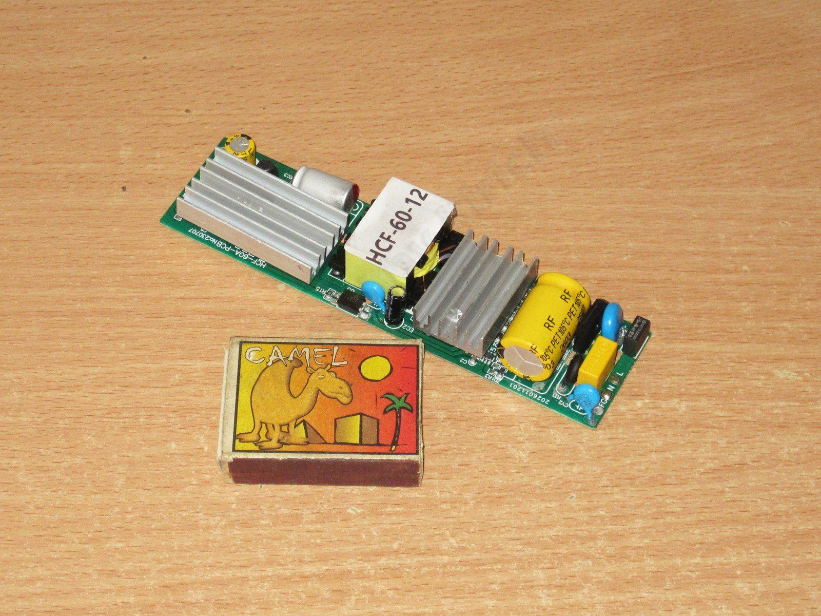
The high-voltage transistor and output diode assembly are cooled by heatsinks. Of course, they’ll behave differently when potted, but the basic point remains: even through the potting compound, heat will be dissipated better than with a diode mounted directly on the board, as in the 36 W and 40 W versions.
Though it’s quite possible that heat will be dissipated even better this way than in open air.
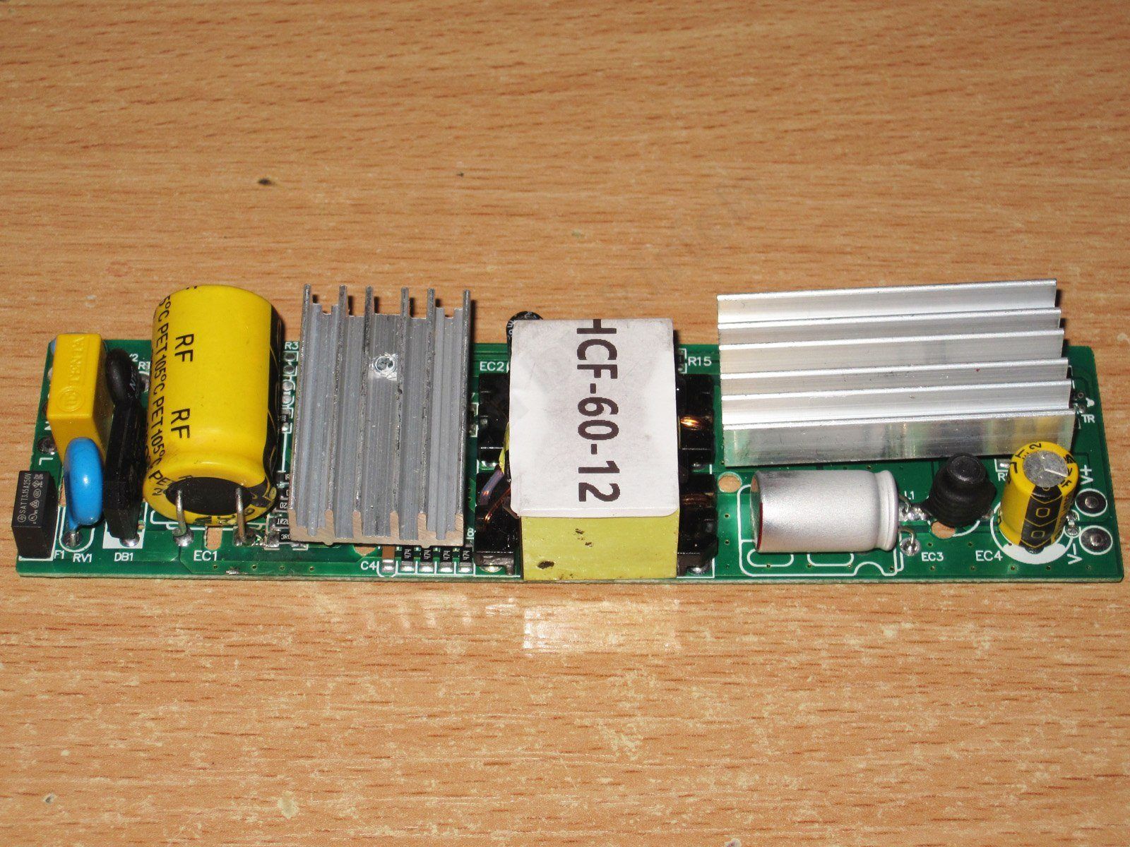
There’s no input filter here, and none is even provided for, but all the other necessary components are present, including a varistor and thermistor. The varistor is also installed correctly here, after the fuse.
The input capacitor is 68 µF.
The shunt resistors made me laugh. I understand this is a prototype, but they look pretty funny :)
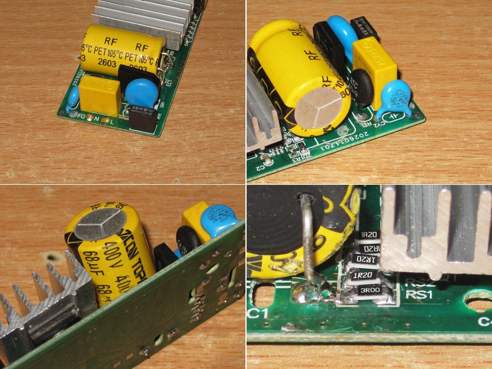
The Y capacitor and the PWM controller’s supply capacitor are also marked Rubycon.
The output winding uses several wires.
The output stage is better here: first, there’s a 2200 µF polymer capacitor; second, there’s an inductor after it, followed by a regular 680 µF capacitor. Replacing the regular capacitor with a polymer one was our requirement.
No safety concerns.
The input capacitor’s actual capacitance is about 62 µF, and the output capacitors total 2600 µF. That’s perfectly fine for a 230 V mains supply; at 115 V, it’s better to reduce the load below the maximum.
The protection is set to trip at 6.1–6.3 A, both cold and hot. Excellent, in my opinion.
Ripple with no load and at currents of 2, 4, and 5.5 A.
I think 40 mV even at maximum load is pretty good.
There’s some strange 100 Hz ripple at low frequencies. I’ve written before that it may be a quirk of the PWM controller used here. In this case, though, it’s not particularly critical because the ripple’s peak-to-peak amplitude is small.
This is a feature of the overload protection. You saw that when the threshold is reached, the PWM controller reduces the voltage rather than shutting off the load.
I don’t recommend pushing the power supply into this operating mode.
On the left, low-frequency ripple at 5.9 A; on the right, at 6 A. You can see that when the power supply starts entering protection, it goes haywire.
The thermal test was done in two stages, at 2.5 A and 5 A, for a total of over an hour. The voltage is practically unaffected by temperature or load.
At 2.5 A, the transformer reaches 50 degrees, the transistor 49, and the diode assembly 61.
At 5 A, the transformer reaches 71 degrees, the transistor 68, and the diode assembly 96.
As you can see, in this configuration the power supply has a decent amount of headroom—at least 20–25 degrees. Potting it will change things a little, but I don't think it will change much; and besides, it's hard to say which way things will go. I'd expect it to be better.
HCF-100-12 power supply: 100 W, 12 V, 8.3 A — link
This one is even closer to the real-world setup. The only difference from the finished version is that it hasn't been potted. The power supply is still in its original enclosure, which acts as a heatsink. And of course, this affects the final component temperatures. It's fairly difficult to predict exactly how, since the potting compound doesn't cool anything; it just spreads (equalizes) the heat across the enclosure. So some components will fare better, and others worse.
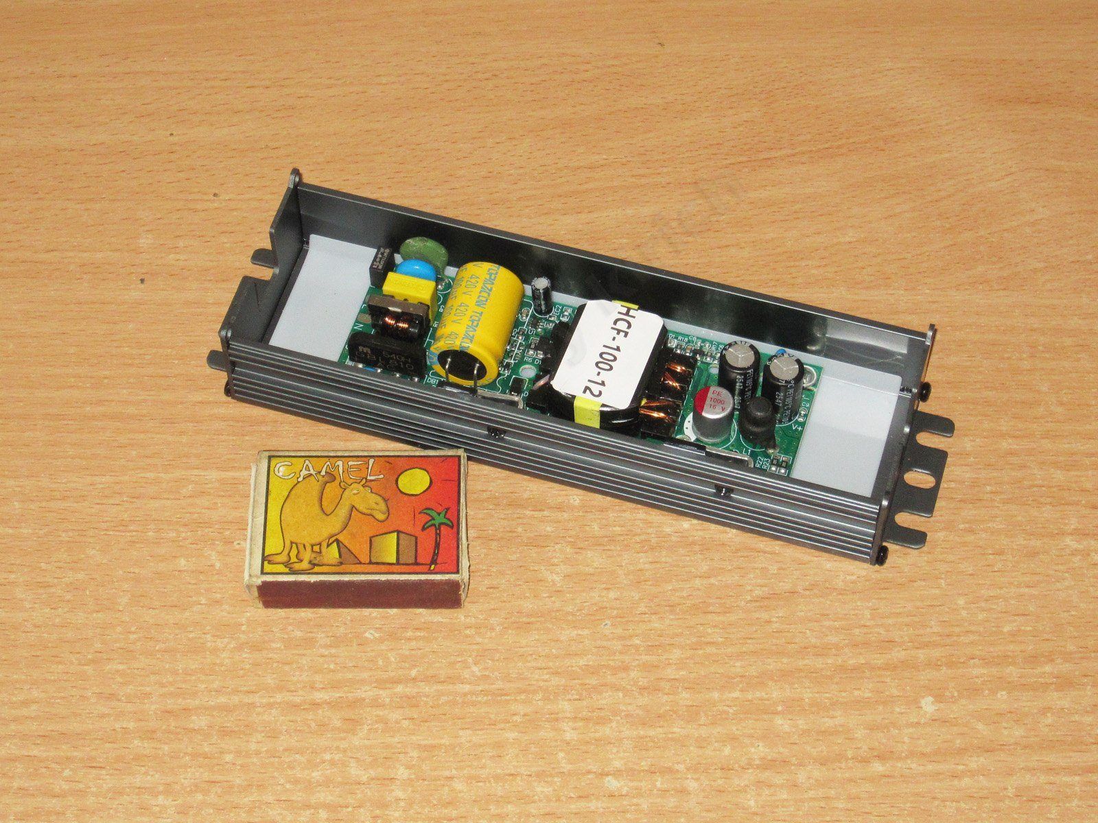
The board is noticeably smaller than the enclosure, so I think it should cool even better once potted.
I have no complaints about the build quality, and for some reason I just like this power supply.
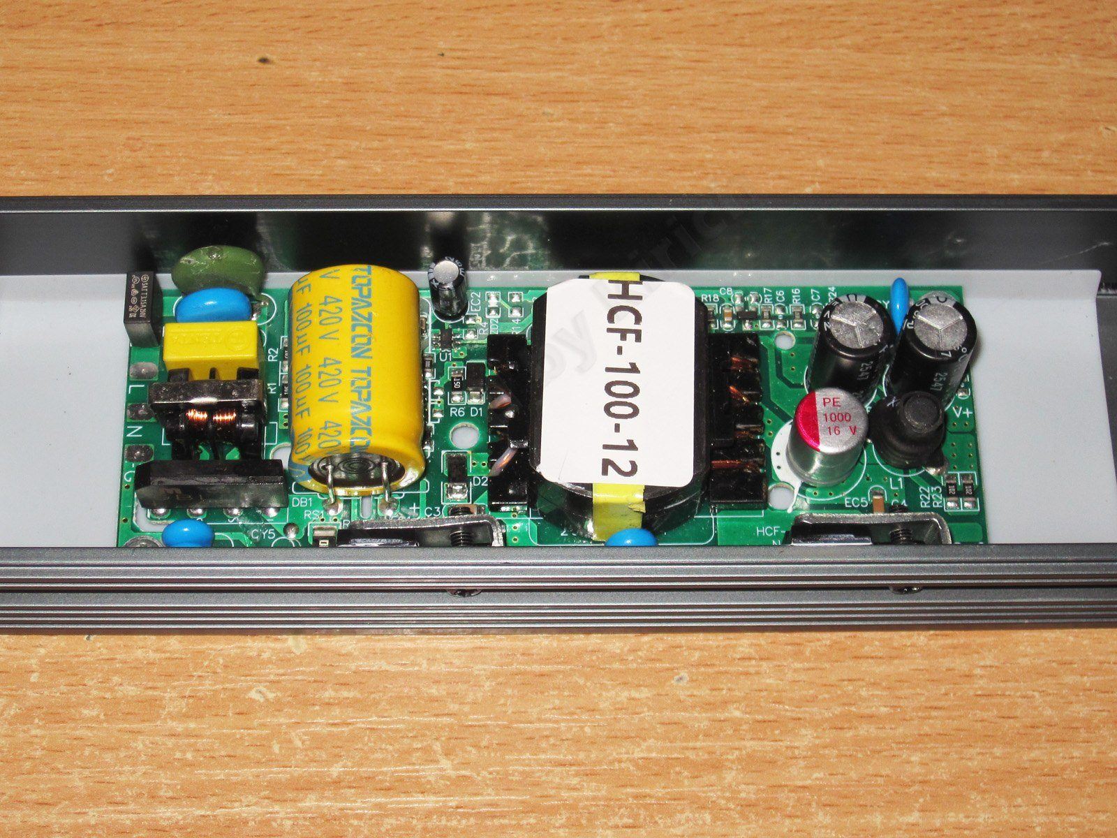
1. The input already has a proper filter, as well as a varistor, thermistor, and several Y capacitors.
2. As expected, the transistor is mounted with thermal paste. A 200 mΩ shunt is visible nearby.
3. PWM controller. There's a spot nearby for the MOSFET driver transistors, but they're not used in this version.
4. The output has two standard capacitors and one polymer capacitor, plus an inductor to reduce ripple. The inductor is clearly rated for a fairly high current.
5. All the capacitors are 1000 µF, and the diode assembly is also mounted with thermal paste.
6. One thing that surprised me when I started checking it: there are no contact pads for connecting the output cable. So I soldered it to the spot where the output ceramic capacitor was supposed to go :)
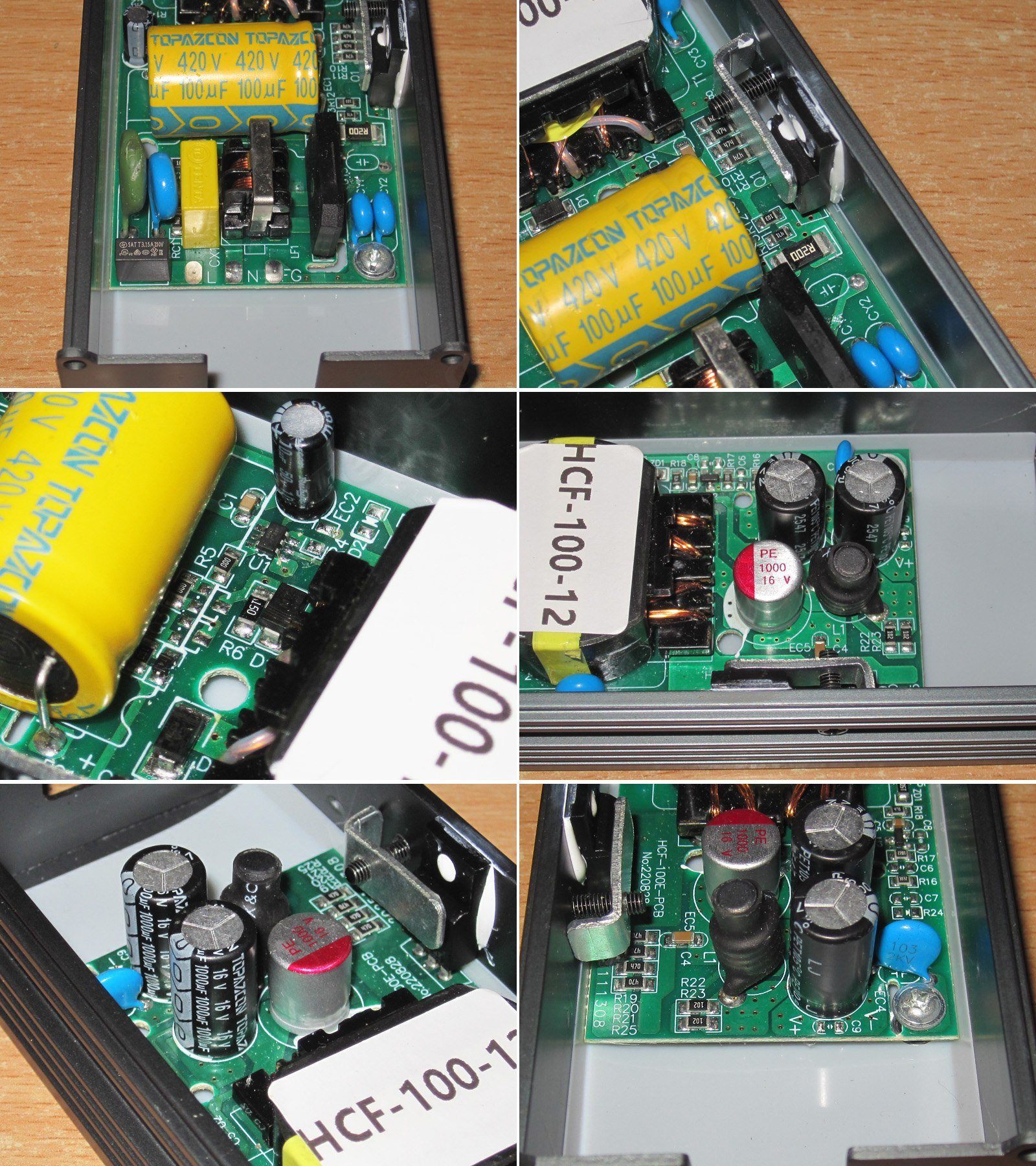
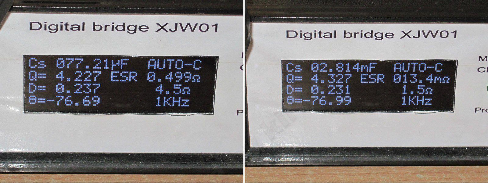
The actual input capacitor capacitance turned out to be noticeably lower than specified: it's rated at 100 µF, but measures about 77. At the usual 230 V, this isn't particularly critical, of course—it'll work just fine—but it's a little disappointing.
The output is closer to spec: 2800 µF, ESR 13.4 mΩ. No complaints there.
When I tried to determine the protection trip current, I hit the limit of my electronic load, which is 10 A, both cold and hot.
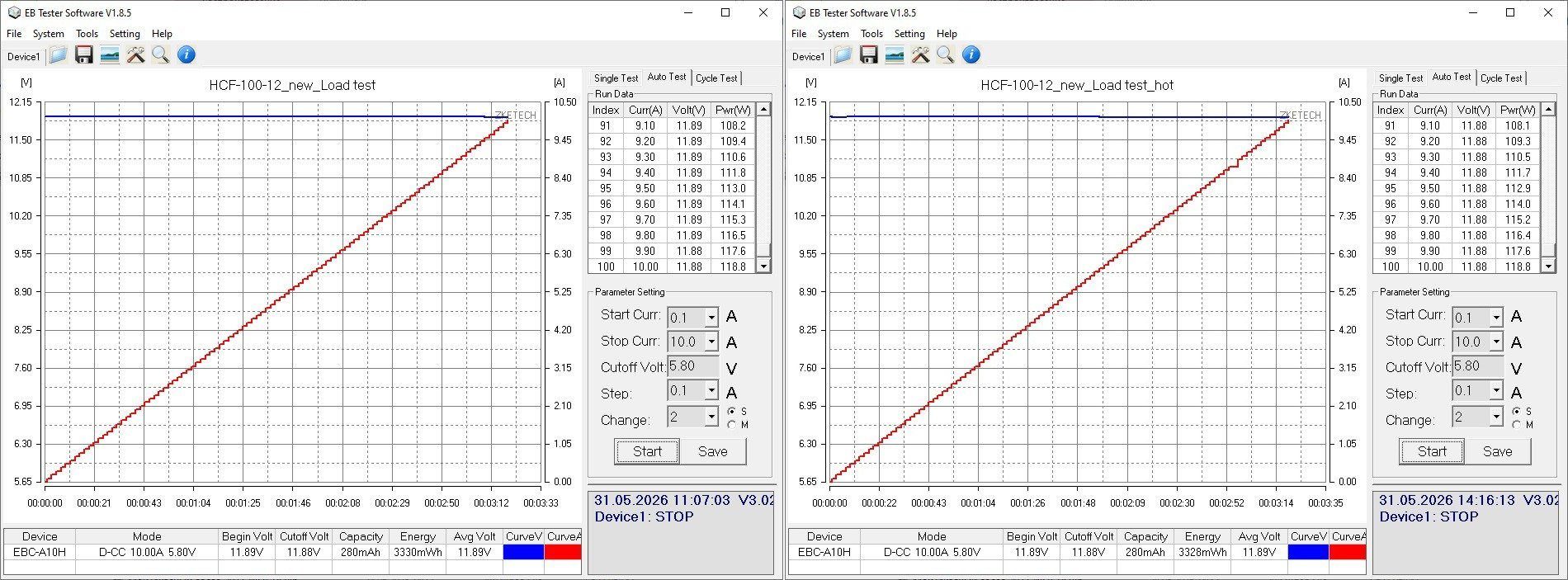
The test showed, first, that the protection is set to about 10.5 A, and second, that the power supply reduces its voltage as the load increases—in effect, it switches to a mode close to constant-power regulation.
This is a little debatable. I might have used a 220 mΩ shunt instead of 200 mΩ, which would bring the protection current down by about 10%, but overall it's not critical.
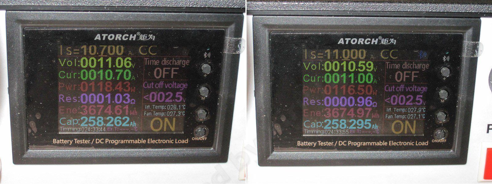
Ripple at no load and at 3, 6, and 9 A looks excellent here too: just 30 mV even at the heaviest load, and essentially no "spikes".
Ripple at the mains frequency is also fine, and given the overall level, it's excellent.
The temperature test was run at 4.2 and 8.4 A, roughly 50% and 100% load. Then I added another stage at 10 A, i.e. 20% above the maximum.
The voltage varies slightly with the load, by just 20 mV, and shows no noticeable dependence on temperature.
And here are the results.
4.2 A — transformer at 63 degrees, transistor at 42, diode assembly at 48
8.4 A — transformer at 98 degrees, transistor at 59, diode assembly at 75.
10 A — transformer at 115 degrees, transistor at 71, diode assembly at 87.
The only real concern is the transformer temperature. But keep in mind that once it’s potted, the heat will be distributed more evenly, so the temperature will probably drop a little. It should be able to deliver its rated 100 W continuously without any problems.
Model HCF-150-12, 12 V, 150 W, 12.5 A — link.
This model is very similar to the previous one, but scaled up for higher power.
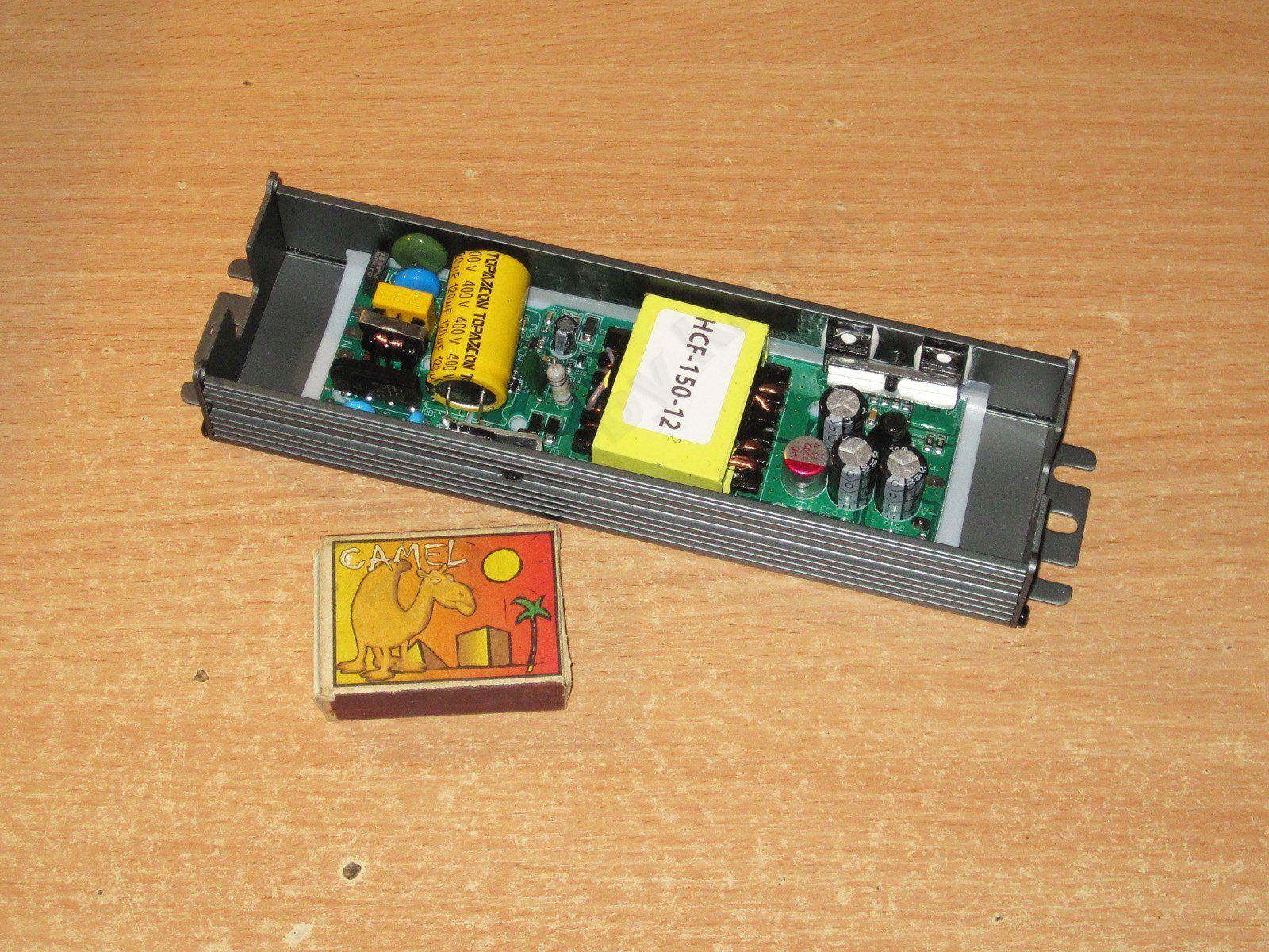
The layout is practically unchanged, with a few minor tweaks. Basically, they took the 100 W power supply, replaced the key components with higher-power ones, increased the capacitor capacity, added another diode assembly, and ended up with a 150 W power supply.
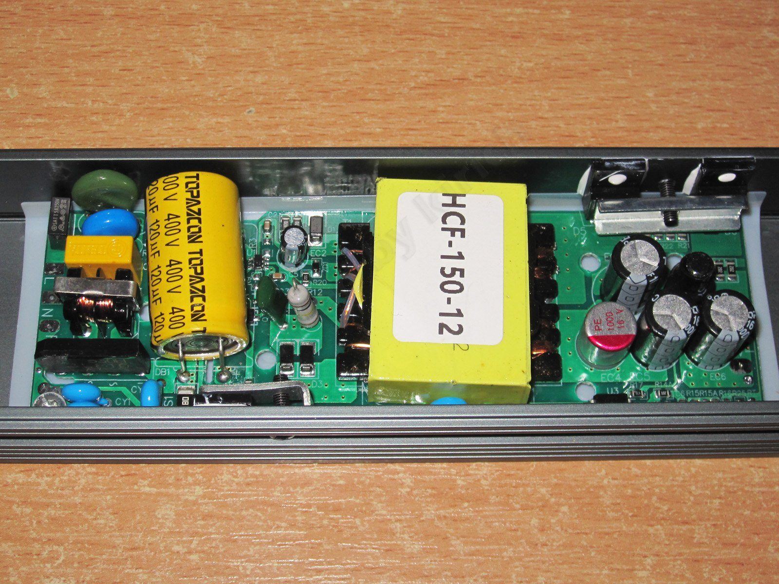
1. It also has an input filter, varistor, thermistor, etc. The input capacitor is rated at 120 µF.
2. PWM controller section; the snubber components are also visible here.
3. The transistor is held against the heatsink with thermal paste.
4. The transformer winding uses Litz wire—nice.
5. There are two diode assemblies in parallel on the output; I approve.
6. There are four output capacitors: three standard ones and one polymer capacitor, all rated at 1000 µF. There’s also an inductor to reduce ripple.
The input capacitor measures about 105 µF, which is acceptable for 230 V, though I’d like to see more; it’s too little for 115 V.
The output capacitance measures about 3900 µF, which is practically what’s specified. ESR is 10.6 mΩ, 30% lower than in the 100 W version. Good.
It looks like the same PWM controller is used, since the power supply behaves the same as the 100 W version when it comes to protection: it doesn’t shut down, but reduces the output voltage. The threshold is set to about 14 A; at 14.7 A, the output is already down to around 10.8 V.
For the rated current of 12.5 A, I’d lower it a little, but overall it’s perfectly fine as is and can be left alone.
Ripple with no load and at currents of 4, 8, and 13 A.
The main part is practically unchanged: we get about the same 30 mV as with the 100 W version, which is good. But there are now “spikes.” They’re not critical, and the overall amplitude is small. Still, something tells me that in this case, as well as based on measurements of the previous model, this may be a quirk of the circuit board layout.
In any case, the overall verdict is very good.
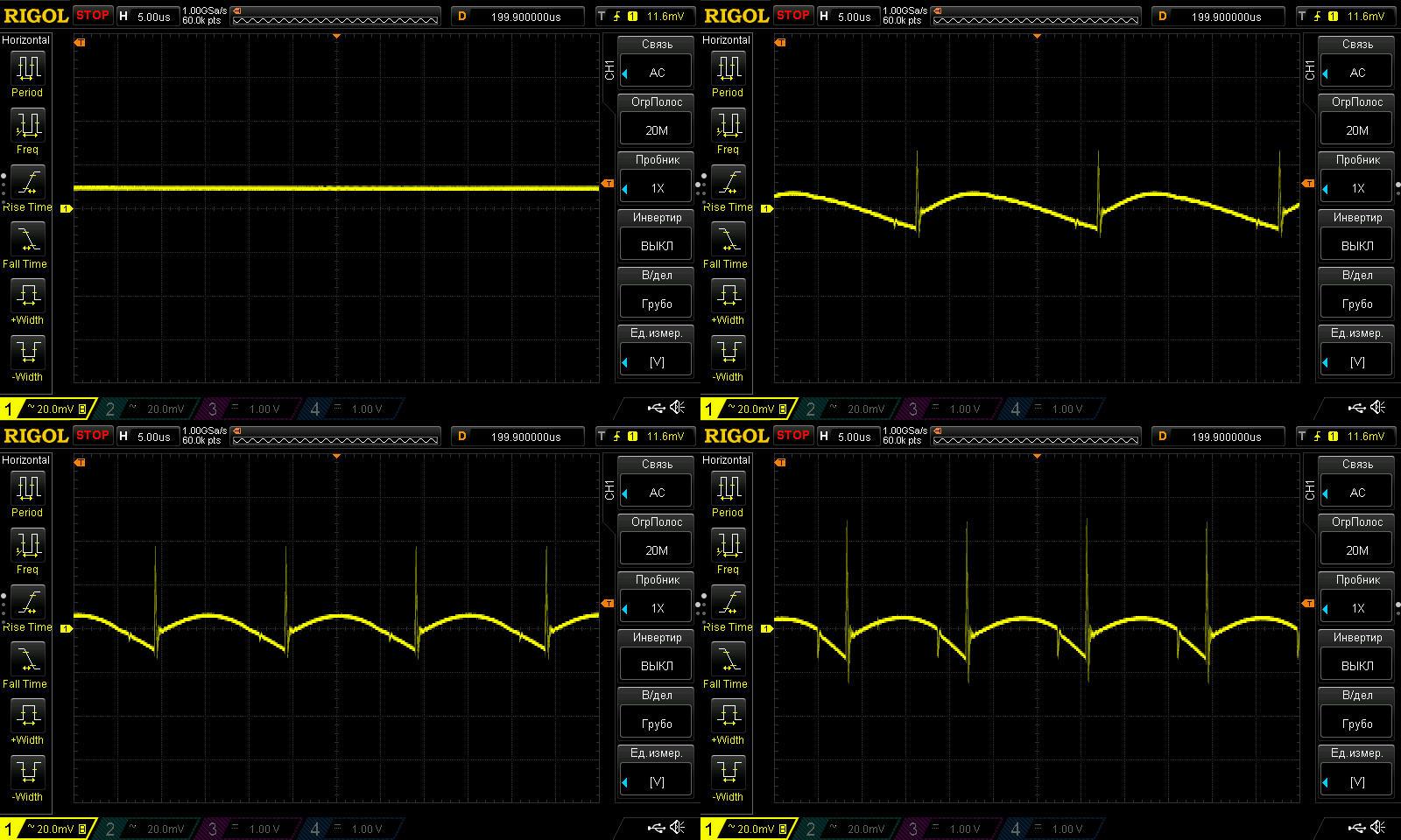
At low frequency, the waveform is predictably worse than on the 100 W version. But even here, the total amplitude is only around 60 mV, so I have no complaints.
The temperature test was run in three modes: the rated 6.5 and 12.5 A, plus an additional test at 14 A, i.e. at the maximum protection setting.
The first two stages lasted about 25–30 minutes each, and the third ran longer, almost 50 minutes, so I consider the test sufficient.
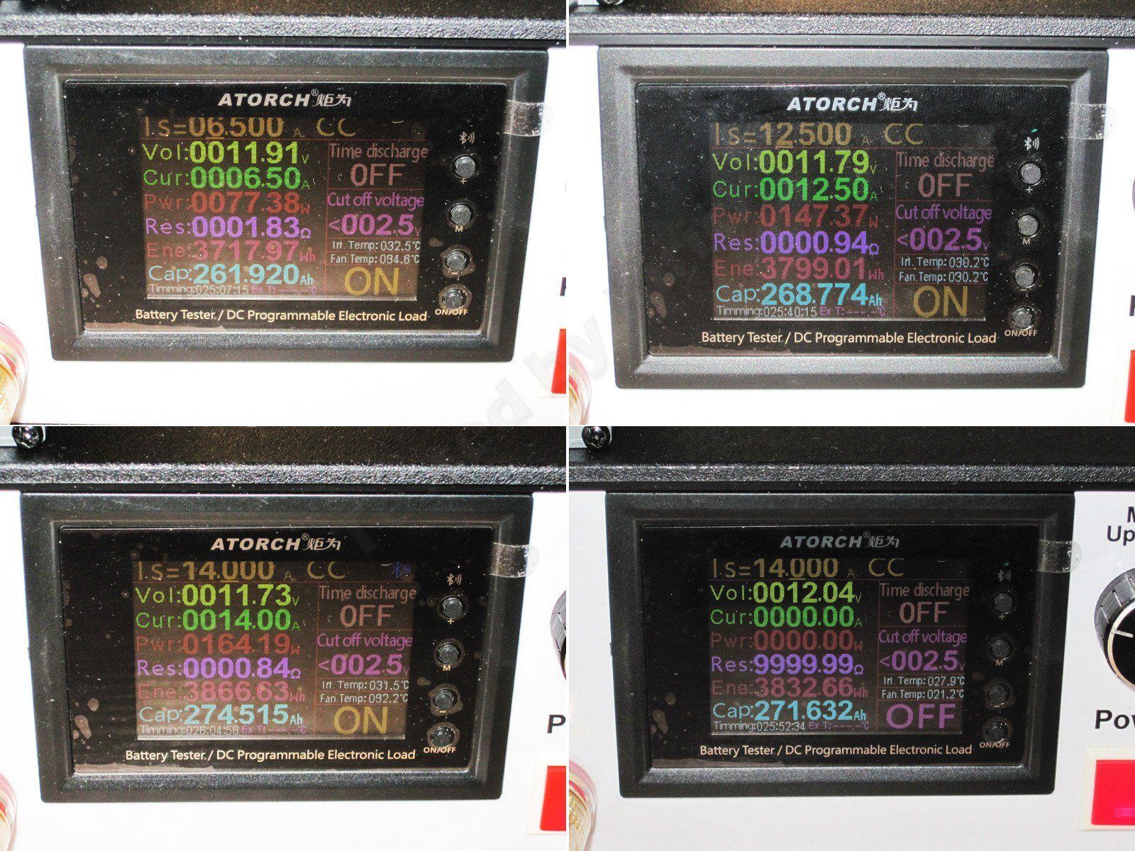
Results:
6.5 A — transformer 64 degrees, transistor 50, diode assemblies 56
12.5 A — transformer 87 degrees, transistor 66, diode assembly 80
14 A — transformer 94 degrees, transistor 75, diode assemblies 90.
Everything looks excellent here. The power supply has plenty of headroom even at the maximum possible 14 A. It definitely warmed up over 50 minutes, and considering it will be potted, that's even better.
There's no point even discussing the normal 12.5 A operating mode; it still has 20–25 degrees of headroom.
Model HCF-200-12, rated for 12 V, 200 W and about 16.5 A — link
This one is more interesting. Although this power supply is only 50 W more powerful than the previous one, it uses a different topology: a half-bridge, used in higher-power designs.
So 150 W was the upper limit for flyback converters, while this one is at the lower end for half-bridges. It'll be interesting to compare them.
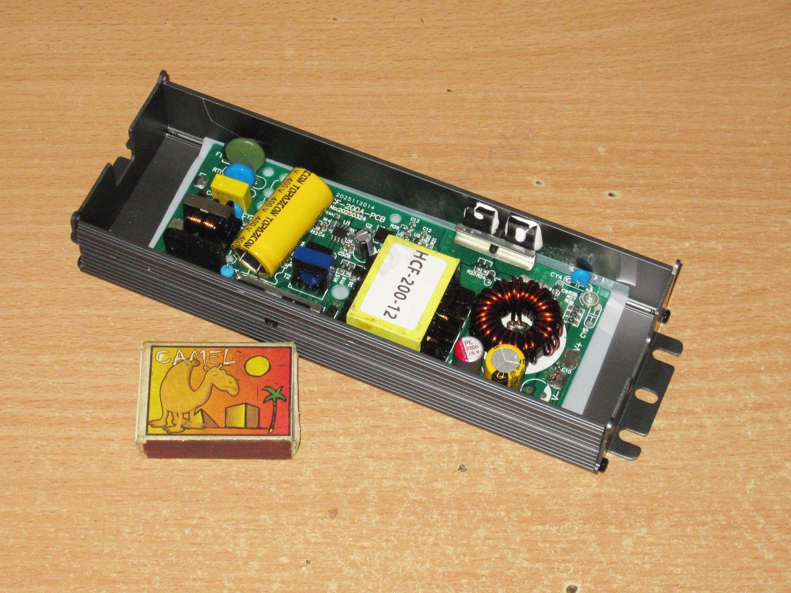
The circuit design is different, and the layout is somewhat similar, but the large output choke stands out immediately, along with the isolation transformer used to drive the transistors.
1. A full input filter, with an input capacitor rated at 150 µF.
2. As in all the previous models, there's a 560 V varistor, rated for peak voltage. Its purpose is essentially to protect against short high-voltage spikes.
3. The PWM controller section. You can also see that the transistors are mounted with thermal paste. PWM controller: NCP1252.
4. The current-sense shunt gave me some pause early on, so I asked to have it replaced with a higher-power one.
5. There are two diode assemblies on the output, but unlike the previous models, they aren't connected in parallel; each one is in its own leg.
6. There are two output capacitors, both 2200 µF: one standard, the other polymer. The polymer capacitor is really just there as an extra precaution, since the topology means the capacitors operate under less stress than in the previous models.
The input capacitor's actual capacitance is 127 µF. That's a little low, but not excessively so. This topology only operates over a narrow range—in this case, 230 V—so it doesn't need a large capacitance. Even Mean Well units have a similar capacitance.
For example, a 200 W Mean Well with the same topology has a 165 µF capacitor. What bothers me more is that it’s rated for 150, which is perfectly reasonable, but in reality it’s 127 :(
The output capacitance is about 4100 µF, which is more than enough for these operating conditions.
Overload protection completely shuts off the output for a while. The trip current is about 20.7 A.
Ripple with no load and at currents of 6, 12, and 18 A.
The main ripple is around 50–60 mV, but there are some pretty pronounced “spikes.” In the vast majority of cases, the load won’t care about them, and most of them will be filtered out by the cable anyway.
But there’s something odd here, because this topology usually has almost no output ripple at all, especially considering that there’s a polymer capacitor on the output. Mean Well doesn’t use polymer capacitors in its LRS200, LRS350, or even more powerful models, though the conventional capacitors it does use are very good.
Overall, my personal opinion is that the PCB layout isn’t quite optimal somewhere.
At low frequencies, the total noise amplitude is about 300–350 mV, most likely because of those spikes. But the 100 Hz component is almost absent, which is good.
The test was run in three modes: the two main ones, at 10 and 17 A, plus an additional 17-minute run at 18 A.
10 A — transformer 51 °C, transistors 43 °C, inductor 55 °C, diodes 56 °C
17 A — transformer 73 °C, transistors 60 °C, inductor 90 °C, diodes 87 °C
18 A — transformer 78 °C, transistors 64 °C, inductor 95 °C, diodes 93 °C.
It’s already clear that even with a 10% overload, at 18 A, the power supply performs very well. The main components have some headroom, and there are certainly no problems at 17 A, even though the rated maximum current for this model is 16.5 A.
I wasn’t too happy with the shunt temperature, though: about 110 °C at an output current of 18 A. So I recommended either adding a second shunt of the same power rating in parallel, or replacing it with a single, higher-power one.
Otherwise, no complaints.
HCF-250-12 power supply, 250 W, 12 V, 21 A — link
This is essentially a more powerful version of the previous model, but I liked it more even at a quick glance. That said, judging anything by appearance alone is pretty pointless.
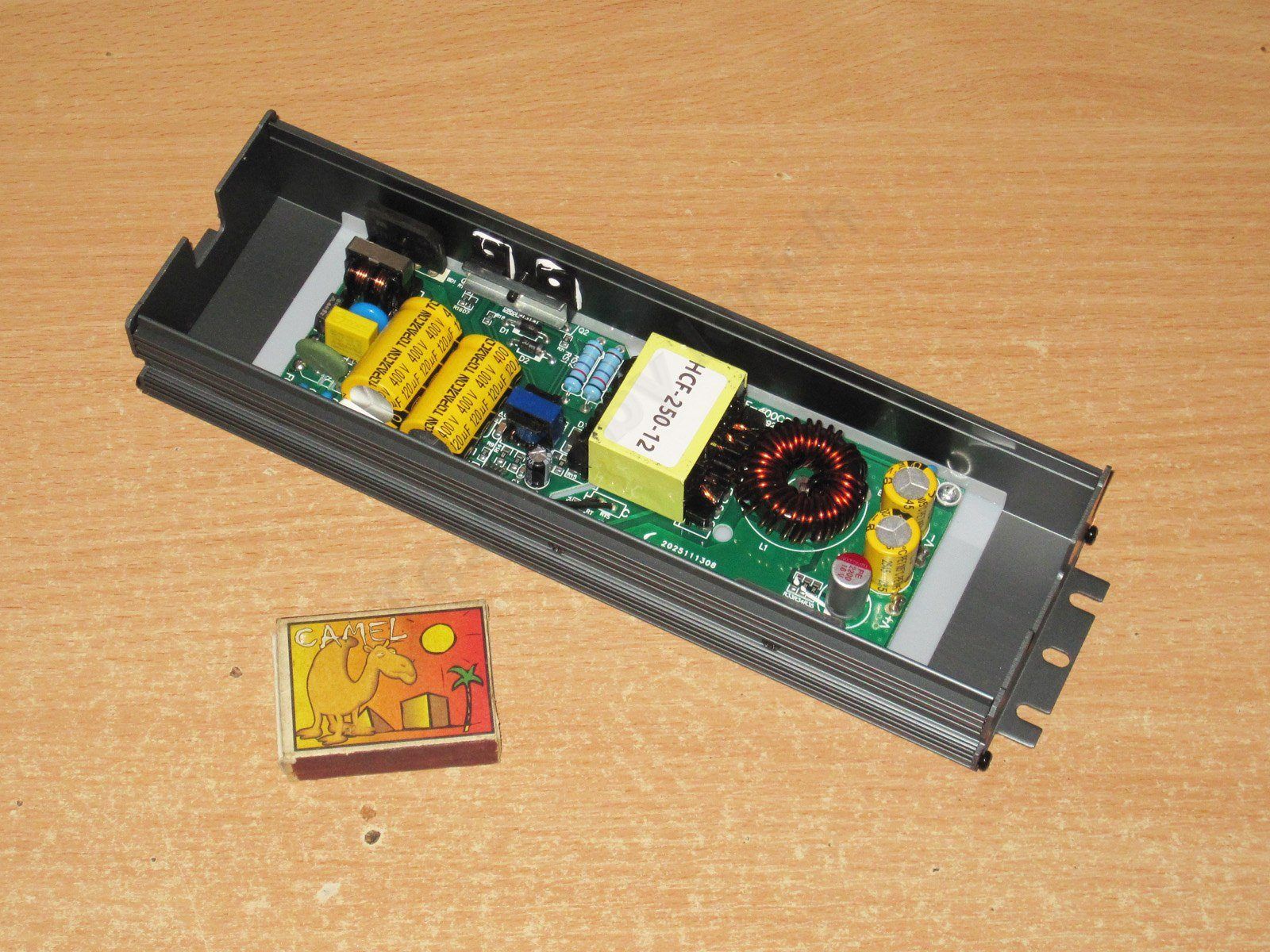
There are now two input capacitors and two shunts, while the output has three capacitors instead of two.
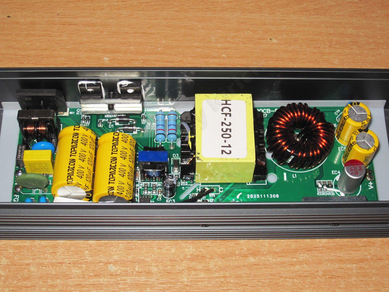
1. Input filter
2. A pair of input capacitors rated at 120 µF; the thermal protection relay is also visible here
3. Transistors mounted with thermal paste; as I mentioned, there are two shunts here.
4. The winding is made from stranded wire, although there aren’t many strands, which is a little odd
5. There are three output diode assemblies. I’ve mentioned before that this topology has “upper” and “lower” diodes, which heat up differently. I think the pair installed here are the ones that run hotter.
6. Output inductor and filter capacitors: one 2200 µF polymer capacitor and a pair of conventional 2200 µF capacitors.
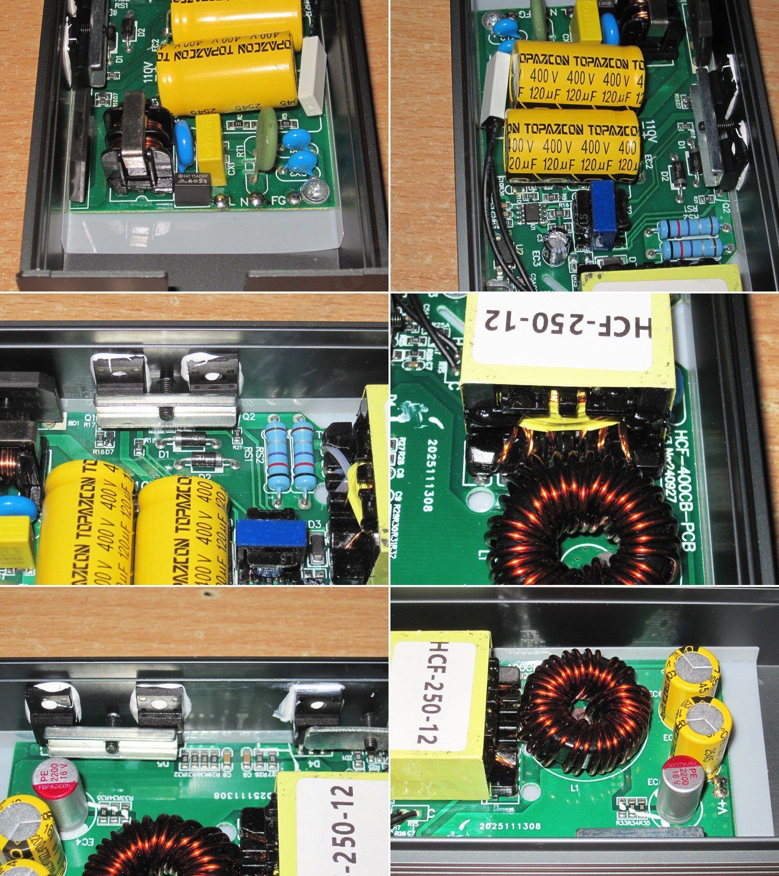
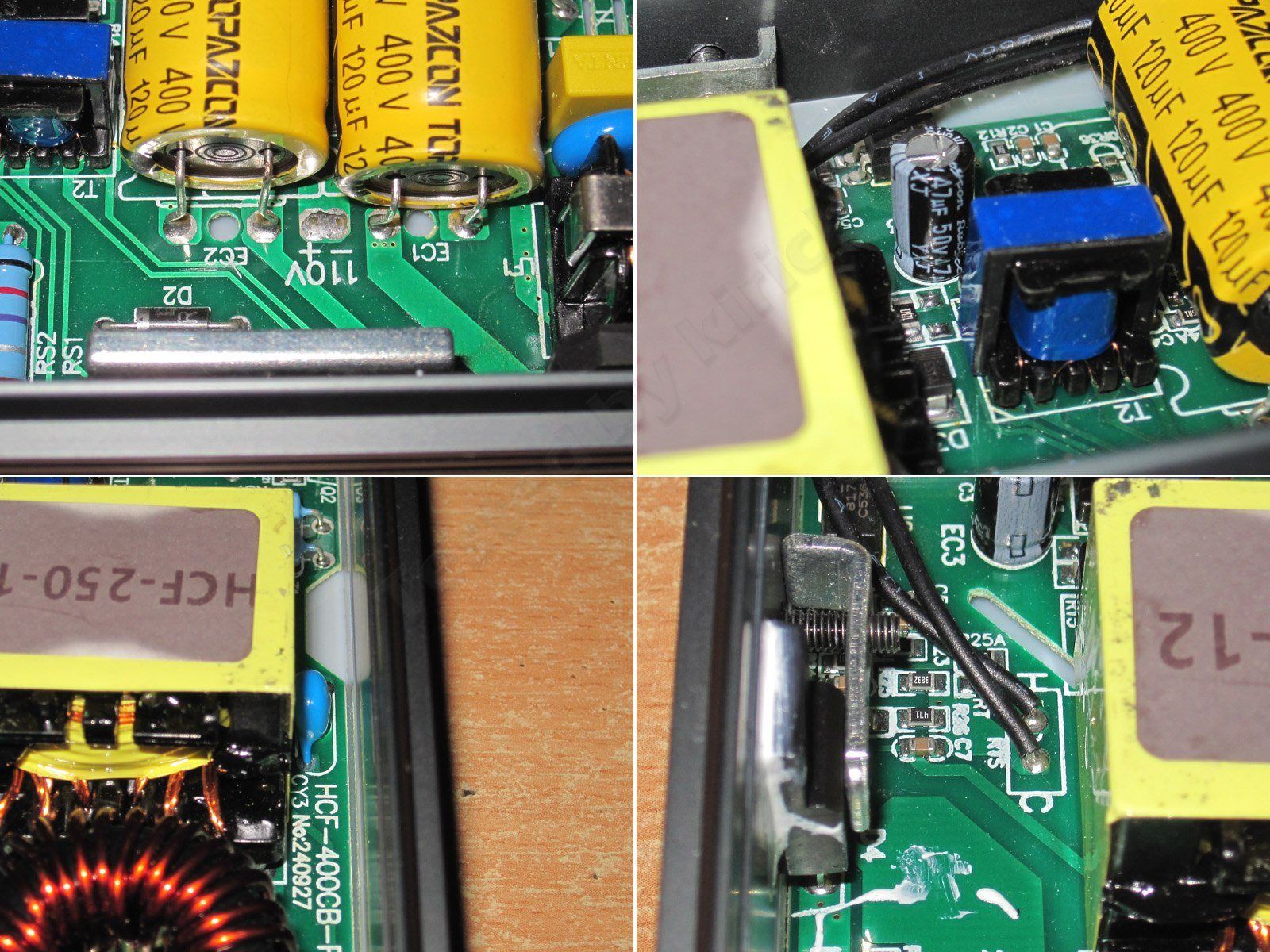
1. Judging by the markings, the capacitors can be configured for 115 V mains, most likely using jumpers.
2. The PWM controller’s supply capacitor is marked Rubycon. We asked them to use high-quality parts, possibly even genuine ones.
3. The Y capacitor is tucked between the transformer and the case.
4. An interesting implementation of overtemperature protection. The thermal protection is connected to the feedback circuit, so when the power supply overheats, it doesn’t shut down completely but reduces the output voltage. I think I’ve shown this before. It’s a very good solution for lighting systems: in the event of a fault, the lights won’t go out completely; they’ll just get noticeably dimmer.
In reality, the input capacitance is about 205 µF, which is perfectly reasonable for 250 W. The output capacitance is about 6250 µF, which is also more than enough for this topology and these specifications.
I did have an issue with the protection current being set much too high: the power supply easily delivers 28 A (331 W) despite being rated for 21 A, 250 W. Beyond that, it simply reduces the voltage, but keeps running even with 30 A at the output, delivering 300 W.
I passed this feedback on to the manufacturer, and they started saying something along the lines of: if we lower the protection current, it will shut down much sooner. So, we’ll need to investigate this further, because 28 A is a lot.
Ripple with no load and at currents of 7, 14, and 21 A.
Here we see the characteristic output waveform of a power supply with this topology. The peak-to-peak ripple is only about 85 mV even at 21 A, which is very good. There are also almost no “spikes,” which is another plus.
There’s a little 100 Hz ripple visible at the low end, but only a little, and it’s easy to ignore.
Just out of curiosity, I checked the output at 27 and 28 A.
At 27 A, the ripple has increased, but it’s mostly the low-frequency component that has risen, along with the overall waveform. At 28 A, though, the power supply starts going into protection, and we can see fairly large low-frequency ripple.
On the other hand, even this “large” ripple is only about 200 mV, which is considered normal for quite a few power supplies.
In any case, if your power supply has a gradual rather than stepped protection response, try not to bring the load too close to the trip threshold.
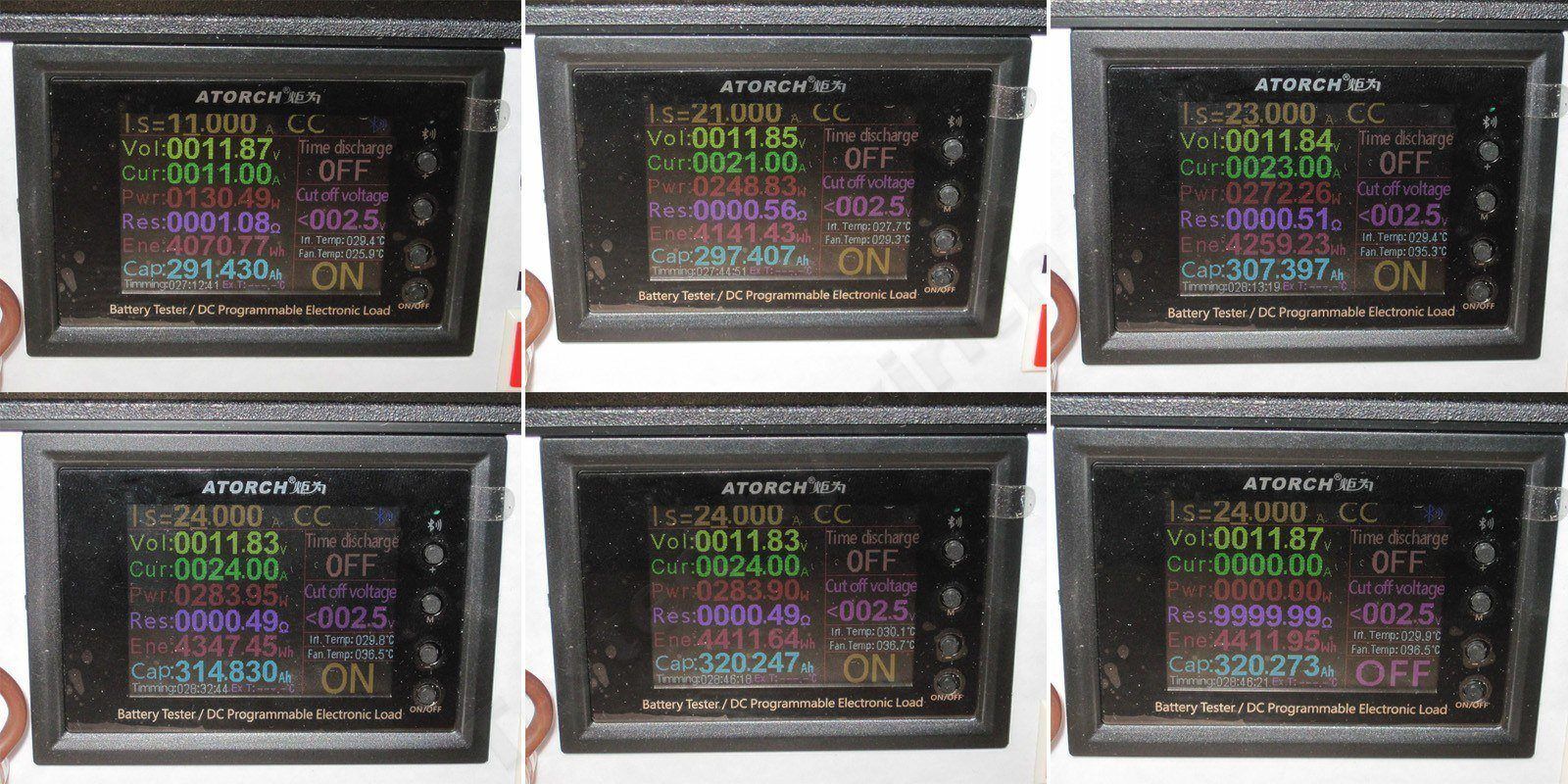
The temperature test was carried out in four stages, at currents of 11, 21, 23, and 24 A. Only the first two are within the rated operating range.
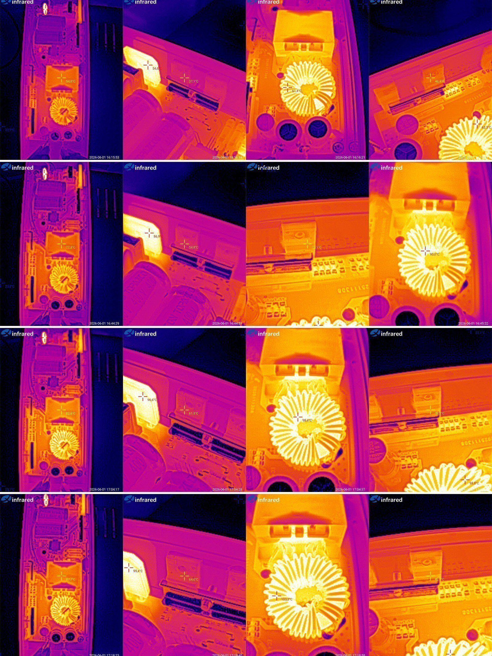
Here are the temperatures of the main components:
11 A — transformer 55 degrees, transistors 37, inductor 61, diodes 46
21 A — transformer 77 degrees, transistors 55, inductor 90, diodes 73 (sorry, I mixed up the last two photos in the series)
23 A — transformer 83 degrees, transistors 61, inductor 98, diodes 78 degrees.
24 A — transformer 88 degrees, transistors 65, inductor 103, diodes 82 degrees.
In my opinion, this power supply performs very well not only within its rated operating range, but also with almost a 15% overload—and that’s without potting it in compound.
Even under overload, there’s a little headroom. The inductor is under the most stress, while the other components are operating in “greenhouse” conditions.
And now, the two most powerful power supplies in the lineup, the HCF-320-12 and HCF-320-24 — link
The models shown are almost identical; the key difference is the output voltage, 12 or 24 V. I’ll start with the 12 V model.
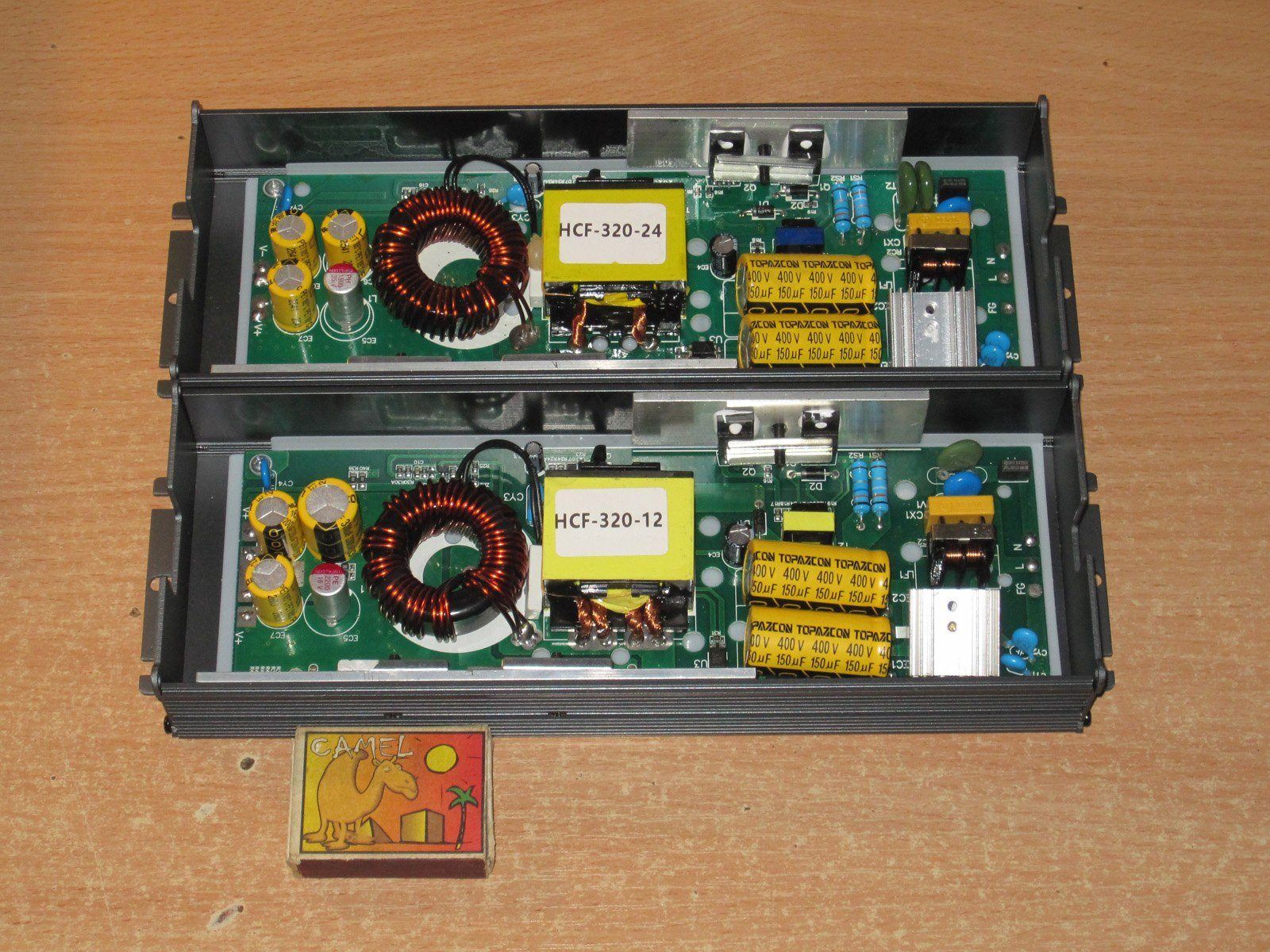
1. A full input filter, a heatsink on the bridge rectifier, and a pair of 150 µF capacitors in parallel at the input.
2. The transistors are clamped down through a heat-spreading plate. I’m not sure there’s thermal paste under the plate, though; the tests will show how it all works.
3. The transformer’s secondary winding is made with fairly thick Litz wire.
4. A thermal protection switch is clamped between the output inductor and the transformer.
5. There are four output diode assemblies, clamped down through a large heat-spreading plate.
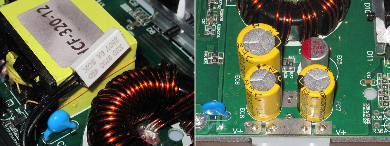
6. An interesting combination on the output: one 2200 µF polymer capacitor and three conventional ones—two 2200 µF and one 3300 µF.
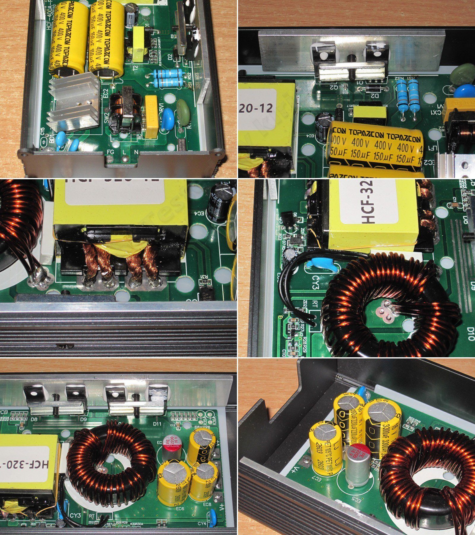
The thermal switch is rated for 80 degrees. The protection works the same way: it reduces the output voltage.
A couple of 2 kΩ ballast resistors are tucked away near the capacitors :)
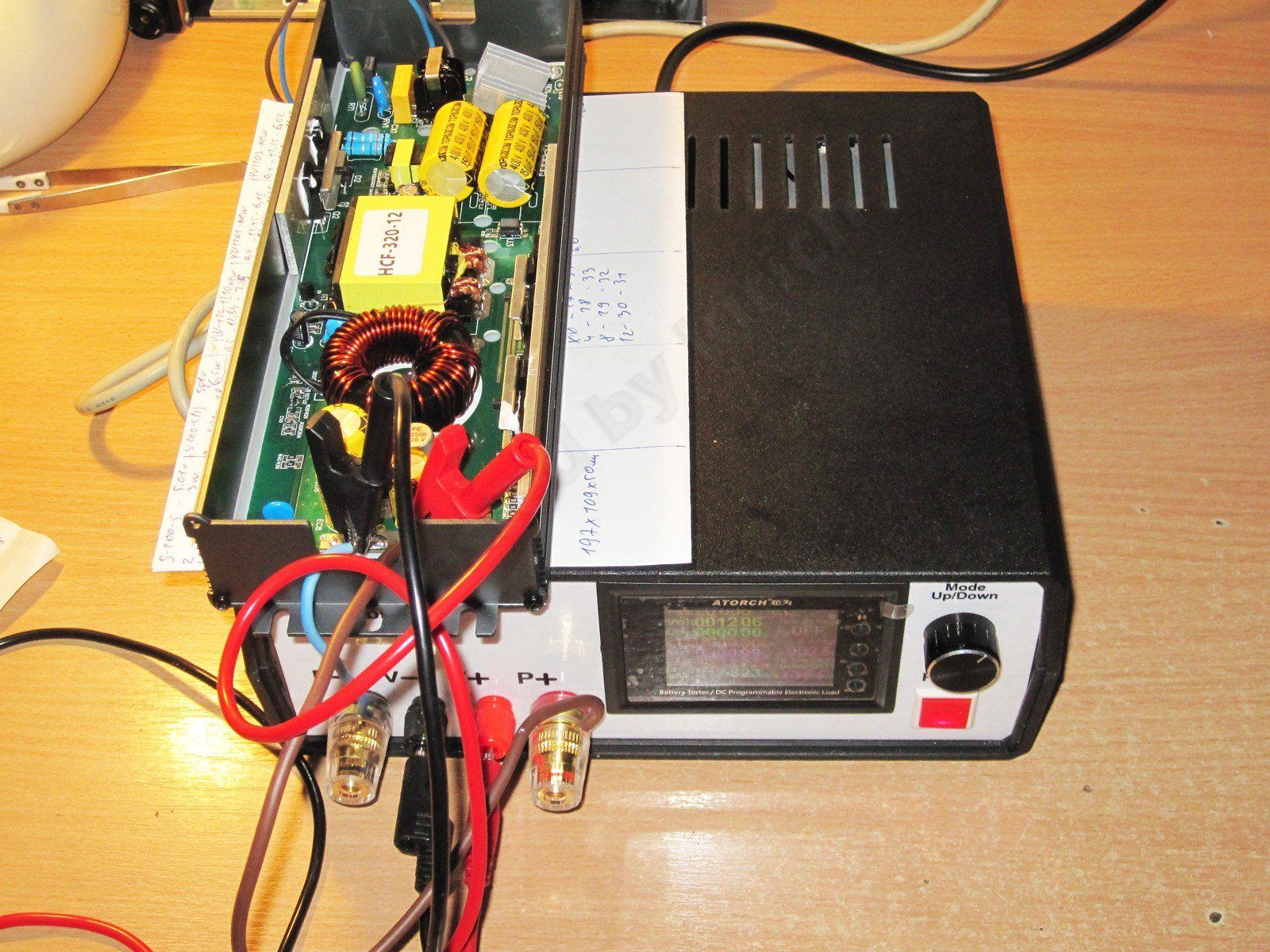
For testing all power supplies rated at 150 W and above, I used a 1200 W load based on Atorch, with a four-wire connection. A reminder: I make electronic loads rated from 1200 to 5400 W, with currents from 50 to 240 A.
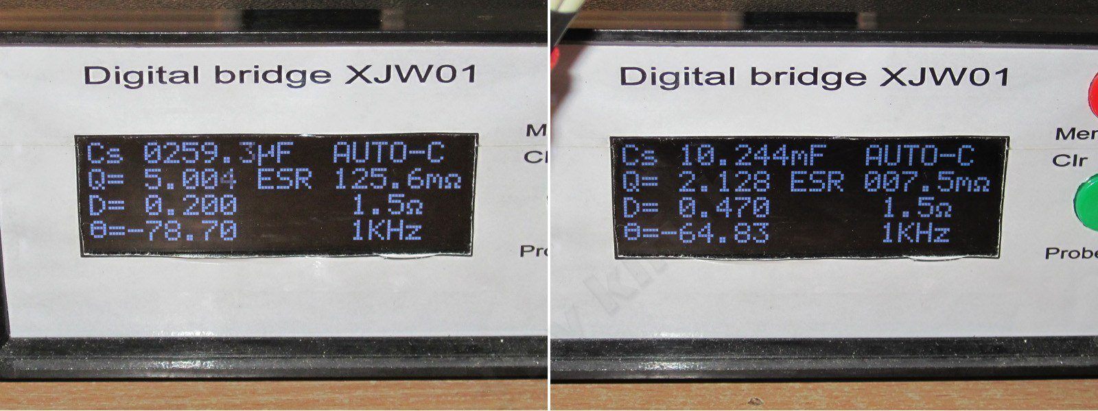
The input filter capacitance is 260 µF, which is fine. As I mentioned, this power supply operates over a “narrow” range, usually 198–260 V.
The output capacitance is 10200 µF, which is more than enough for the specified ratings.
The protection has a fixed threshold and trips at a current of about 30.7 A.
Ripple with no load and at currents of 9, 18, and 28 A.
This is genuinely impressive: even at 28 A (336 W), the peak-to-peak ripple is only up to 40 mV. That’s great.
The low-frequency waveform is just as good—really nice to look at.
The power supply was tested at load currents of 14, 27, and 30 A. Yes, I decided to put it through its paces at 360 W as well.
And now for the component temperatures.
At 14 A: transformer 45 degrees, transistors 42 degrees, inductor 46, and diodes 48.
At 27 A: transformer 70 degrees, transistors 70, inductor 84, and diodes 81 degrees.
At 30 A: transformer 79 degrees, transistors 80 degrees, inductor 95, and diode assemblies 88 degrees.
I think it's obvious that there's even a noticeable margin for operating at 360 W, let alone at 27 A. And that's without potting it with compound, which I think would lower the inductor temperature a little.
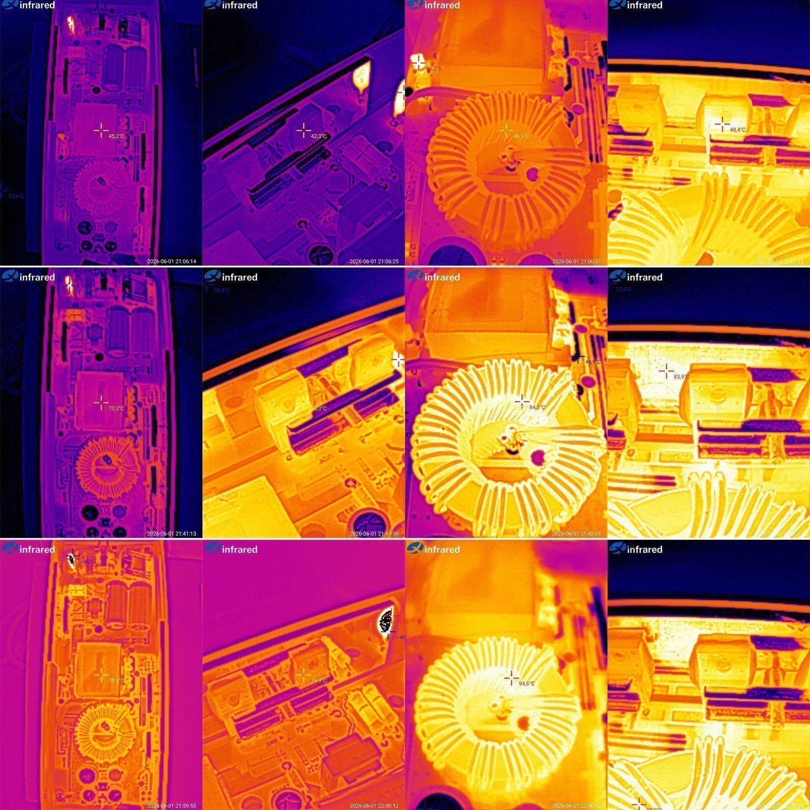
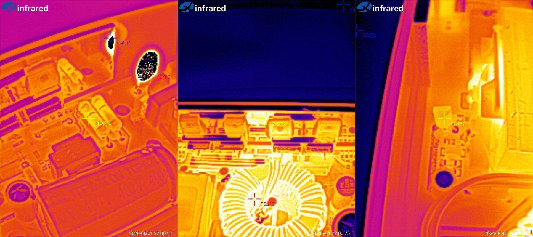
At maximum current, the shunts reach about 100 degrees, which is normal.
As for the diode temperatures, they don't heat up evenly; I measured the maximum temperature at each point.
I noticed some heating of the TL431 zener diode, which is a little puzzling, but the temperature isn't very high—about 77 degrees. It's just higher than I'm used to seeing.
And the 24 V version, HCF-320-24, with a voltage of 24 V and a current of about 14 A — link.
For the most part, I'll be comparing the 12 V and 24 V versions from here on.
The input sections are identical, apart from differences in the PCB layout.
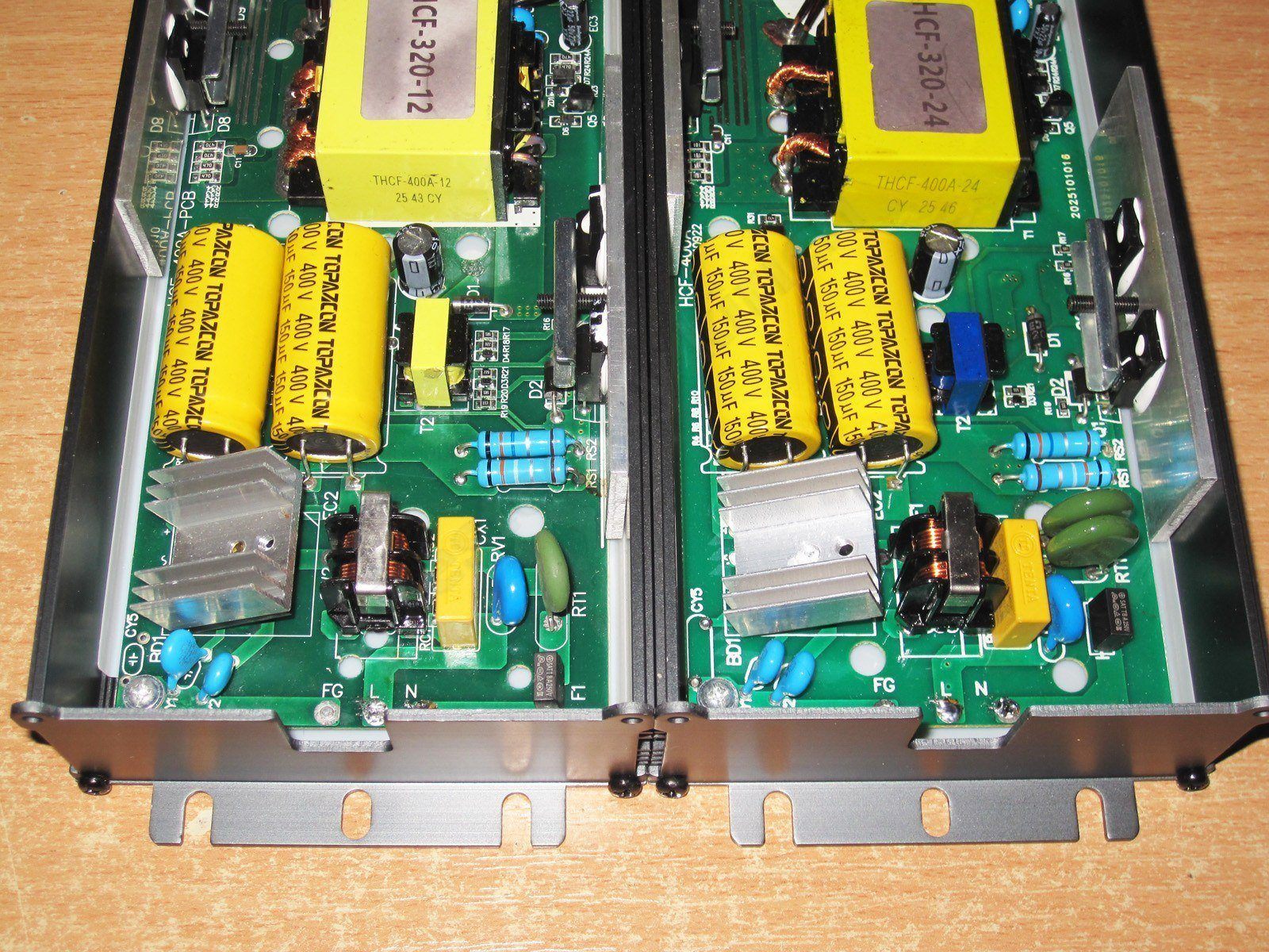
Look closely and you'll see that the boards are different, but the difference is between revisions and has nothing to do with the power supply voltage. The 24 V board is simply newer.
When we pointed out some shortcomings—which, by the way, were more numerous in the 12 V version—we were told that the board was being revised, so the 24 V version is better. As I understand it, they gradually collect suggestions for improvements and then implement them all at once, so there may be another version later that incorporates my suggestions.
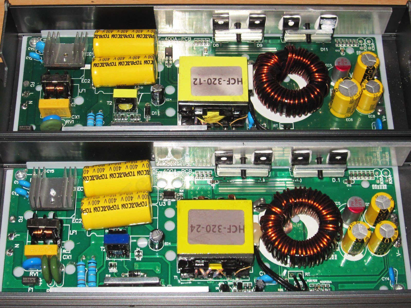
1, 2. The difference between the board versions is visible at the top. You can also see that the optocoupler has already been moved; I haven't thought about why.
3. You can also see that the 24 V board (on the left) looks emptier around the high-voltage section. Perhaps some components have been moved to the underside.
4. On the output, there are 35 V capacitors: one 1500 µF polymer capacitor and three regular 1000 µF capacitors. And yes, the layout of the power planes here is also quite different from the 12 V version.
My concern was the placement of the Y capacitor. Its leads are marked H (hot side) and L (cold side).
You can see that the H lead is quite close to the feedback circuit. With potting compound, this isn't as critical as it would be in an open design, but personally, I don't like either option.
I brought this up with the manufacturer and sent them a photo.
The input filter capacitance is 253 µF. For comparison, the Mean Well LRS-350 has a 280 µF input filter, so they're comparable.
The output capacitance is 4300 µF, which is more than adequate for this topology and a current of around 14–15 A.
The protection is also threshold-based and set to about 15.2 A, which is half the setting of the 12 V version, as you'd expect.
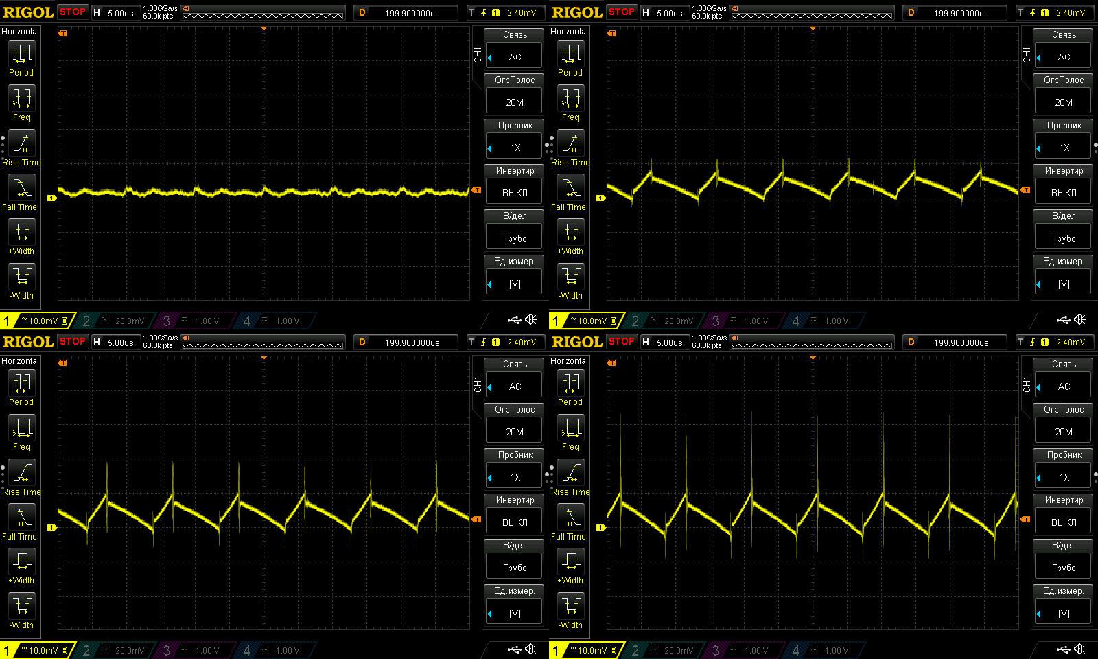
I captured the waveforms with no load and at currents of 5, 10, and 13 A.
Overall, they look good, except for the “spikes,” which I've never liked :)
But in practice, even taking everything into account, the total ripple is about 40 mV, which is negligible given the output voltage. An excellent result.
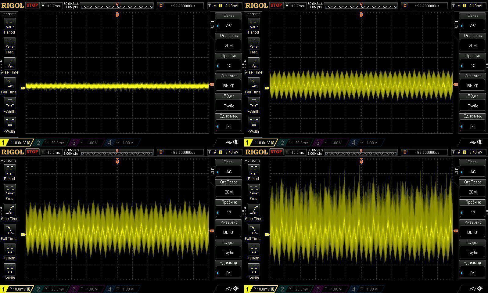
At low frequency, the waveform looks more like “wool,” though it's still excellent here. One division on the screenshot is 10 mV, so this is an excellent result.
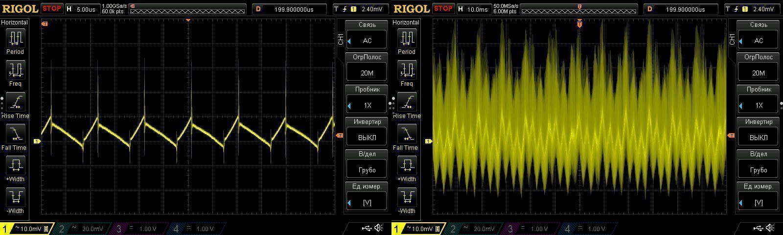
Even when the power supply is loaded right up to its limit at 15 A, the picture doesn't change much. The ripple increases a little, but that's about it.
I checked the temperatures under load in three modes: 7, 14, and 15 A, again at maximum load. That is, The final test at maximum power.
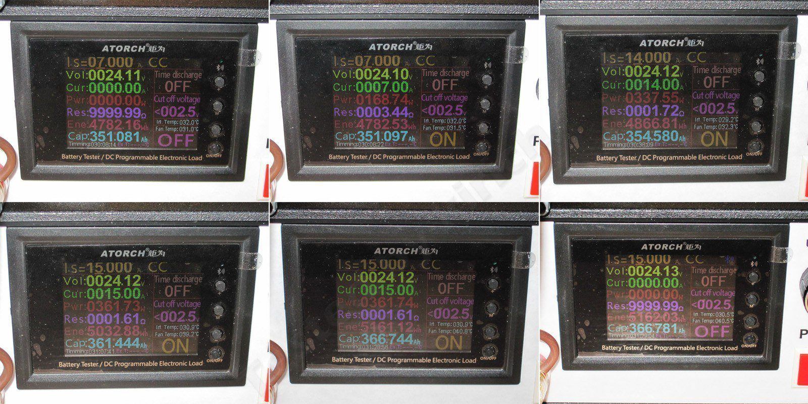
Now for the interesting part: temperatures.
7 A — transformer 50 degrees, transistors 50 degrees, inductor 46 degrees, and diodes 49 degrees
14 A — transformer 79 degrees, transistors 81 degrees, inductor 74 degrees, diodes 73 degrees.
15 A — transformer 86 degrees, transistors 88 degrees, inductor 81 degrees, and diodes 77 degrees.
Interestingly, temperatures here are higher for everything except the inductor than on the 12 V version. The inductor runs cooler, though, so the power supply is better balanced and, even as it is, has roughly 15–20 degrees of headroom.
The bridge rectifier reached 94 degrees, which is also fine. The output snubber got noticeably hot at 114 degrees; I think potting it with compound should help. The capacitors reached 56 degrees, and here the effect will be the opposite: their temperature will rise after potting.
Proper placement of the power components makes quite a difference. The transistors transfer heat to one side of the case, and the diodes to the other, so the case works more effectively as a heatsink than if they were all on the same side.
Conclusions.
HCF-36-12: a small, simple power supply. The main issue is that the varistor is connected before the fuse; that’s not how it should be done.
HCF-60-12: simply a decent power supply, with hardly anything to complain about.
HCF-100-12: the transformer got noticeably hot at 8.4 A and very hot at 10 A, but I think potting it with compound should bring the temperature down.
HCF-150-12: no complaints.
HCF-200-12: a few minor issues with ripple and inductor temperature, but overall everything is within normal limits.
HCF-250--12: no complaints, although the output inductor gets noticeably hot at currents above the rated maximum. At 21 A, everything is fine. The power supply can handle 280 W without a problem, in principle.
HCF-320--12 and HCF-320-24: two great power supplies. I’d say there’s nothing to complain about, but there are a few things. On the 12 V version, the inductor got noticeably hot at 30 A (360 W); I think potting should fix that. There are also some issues with the Y capacitors, or rather, their placement.
One thing almost all these power supplies have in common is low ripple. The exception is the 36 W model, which has no output filter.
I also hope replacing the capacitors will improve reliability, since it has already had a positive effect on ripple.
Overall, all the power supplies performed quite well, especially considering that I tested them not only at their maximum rated operating conditions, but also under significant overload. Even then, I had very few complaints.
That’s all for today. As always, thanks to Vitaly for providing the samples for testing.
This model is included in the summary table: Comparison of power supplies: ripple, efficiency, and temperature rise
The figures from this review are in the measurement database: Power supplies
Calculate manuallyAll calculators
Discounted products
You may be interested in



Discounted products
Support the project
All the content on the site and the advice are free, but we’d be grateful for your support of the project and the channel!
Discuss on the forumHave a question or some experience to share? Discuss the article with the author and readers: the forum is a convenient place to share schematics and photos.
Go to the forumOnly registered readers can comment. It takes a minute to sign up, and you can log in with the same account you use on the forum.
Log inRegister